Microprocessor - 8086
8086 Microprocessor is an enhanced version of 8085Microprocessor that was designed by Intel in 1976. It is a 16-bit Microprocessor having 20 address lines and16 data lines that provides up to 1MB storage. It consists of powerful instruction set, which provides operations like multiplication and division easily.
It supports two modes of operation, i.e. Maximum mode and Minimum mode. Maximum mode is suitable for system having multiple processors and Minimum mode is suitable for system having a single processor.
Features of 8086
The most prominent features of a 8086 microprocessor are as follows −
- It has an instruction queue, which is capable of storing six instruction bytes from the memory resulting in faster processing.
- It was the first 16-bit processor having 16-bit ALU, 16-bit registers, internal data bus, and 16-bit external data bus resulting in faster processing.
- It is available in 3 versions based on the frequency of operation −
- 8086 → 5MHz
- 8086-2 → 8MHz
- (c)8086-1 → 10 MHz
- It uses two stages of pipelining, i.e. Fetch Stage and Execute Stage, which improves performance.
- Fetch stage can prefetch up to 6 bytes of instructions and stores them in the queue.
- Execute stage executes these instructions.
- It has 256 vectored interrupts.
- It consists of 29,000 transistors.
Comparison between 8085 & 8086 Microprocessor
- Size − 8085 is 8-bit microprocessor, whereas 8086 is 16-bit microprocessor.
- Address Bus − 8085 has 16-bit address bus while 8086 has 20-bit address bus.
- Memory − 8085 can access up to 64Kb, whereas 8086 can access up to 1 Mb of memory.
- Instruction − 8085 doesn’t have an instruction queue, whereas 8086 has an instruction queue.
- Pipelining − 8085 doesn’t support a pipelined architecture while 8086 supports a pipelined architecture.
- I/O − 8085 can address 2^8 = 256 I/O's, whereas 8086 can access 2^16 = 65,536 I/O's.
- Cost − The cost of 8085 is low whereas that of 8086 is high.
Architecture of 8086
The following diagram depicts the architecture of a 8086 Microprocessor −
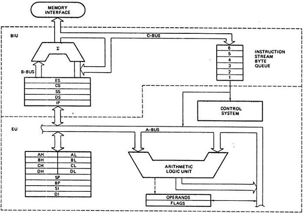
Microprocessor - 8086 Functional Units
8086 Microprocessor is divided into two functional units, i.e., EU (Execution Unit) and BIU (Bus Interface Unit).
EU (Execution Unit)
Execution unit gives instructions to BIU stating from where to fetch the data and then decode and execute those instructions. Its function is to control operations on data using the instruction decoder & ALU. EU has no direct connection with system buses as shown in the above figure, it performs operations over data through BIU.
Let us now discuss the functional parts of 8086 microprocessors.
ALU
It handles all arithmetic and logical operations, like +, −, ×, /, OR, AND, NOT operations.
Flag Register
It is a 16-bit register that behaves like a flip-flop, i.e. it changes its status according to the result stored in the accumulator. It has 9 flags and they are divided into 2 groups − Conditional Flags and Control Flags.
Conditional Flags
It represents the result of the last arithmetic or logical instruction executed. Following is the list of conditional flags −
- Carry flag − This flag indicates an overflow condition for arithmetic operations.
- Auxiliary flag − When an operation is performed at ALU, it results in a carry/barrow from lower nibble (i.e. D0 – D3) to upper nibble (i.e. D4 – D7), then this flag is set, i.e. carry given by D3 bit to D4 is AF flag. The processor uses this flag to perform binary to BCD conversion.
- Parity flag − This flag is used to indicate the parity of the result, i.e. when the lower order 8-bits of the result contains even number of 1’s, then the Parity Flag is set. For odd number of 1’s, the Parity Flag is reset.
- Zero flag − This flag is set to 1 when the result of arithmetic or logical operation is zero else it is set to 0.
- Sign flag − This flag holds the sign of the result, i.e. when the result of the operation is negative, then the sign flag is set to 1 else set to 0.
- Overflow flag − This flag represents the result when the system capacity is exceeded.
Control Flags
Control flags controls the operations of the execution unit. Following is the list of control flags −
- Trap flag − It is used for single step control and allows the user to execute one instruction at a time for debugging. If it is set, then the program can be run in a single step mode.
- Interrupt flag − It is an interrupt enable/disable flag, i.e. used to allow/prohibit the interruption of a program. It is set to 1 for interrupt enabled condition and set to 0 for interrupt disabled condition.
- Direction flag − It is used in string operation. As the name suggests when it is set then string bytes are accessed from the higher memory address to the lower memory address and vice-a-versa.
General purpose register
There are 8 general purpose registers, i.e., AH, AL, BH, BL, CH, CL, DH, and DL. These registers can be used individually to store 8-bit data and can be used in pairs to store 16bit data. The valid register pairs are AH and AL, BH and BL, CH and CL, and DH and DL. It is referred to the AX, BX, CX, and DX respectively.
- AX register − It is also known as accumulator register. It is used to store operands for arithmetic operations.
- BX register − It is used as a base register. It is used to store the starting base address of the memory area within the data segment.
- CX register − It is referred to as counter. It is used in loop instruction to store the loop counter.
- DX register − This register is used to hold I/O port address for I/O instruction.
Stack pointer register
It is a 16-bit register, which holds the address from the start of the segment to the memory location, where a word was most recently stored on the stack.
BIU (Bus Interface Unit)
BIU takes care of all data and addresses transfers on the buses for the EU like sending addresses, fetching instructions from the memory, reading data from the ports and the memory as well as writing data to the ports and the memory. EU has no direction connection with System Buses so this is possible with the BIU. EU and BIU are connected with the Internal Bus.
It has the following functional parts −
- Instruction queue − BIU contains the instruction queue. BIU gets upto 6 bytes of next instructions and stores them in the instruction queue. When EU executes instructions and is ready for its next instruction, then it simply reads the instruction from this instruction queue resulting in increased execution speed.
- Fetching the next instruction while the current instruction executes is called pipelining.
- Segment register − BIU has 4 segment buses, i.e. CS, DS, SS& ES. It holds the addresses of instructions and data in memory, which are used by the processor to access memory locations. It also contains 1 pointer register IP, which holds the address of the next instruction to executed by the EU.
- CS − It stands for Code Segment. It is used for addressing a memory location in the code segment of the memory, where the executable program is stored.
- DS − It stands for Data Segment. It consists of data used by the program andis accessed in the data segment by an offset address or the content of other register that holds the offset address.
- SS − It stands for Stack Segment. It handles memory to store data and addresses during execution.
- ES − It stands for Extra Segment. ES is additional data segment, which is used by the string to hold the extra destination data.
- Instruction pointer − It is a 16-bit register used to hold the address of the next instruction to be executed.
Microprocessor - 8086 Pin Configuration
8086 was the first 16-bit microprocessor available in 40-pin DIP (Dual Inline Package) chip. Let us now discuss in detail the pin configuration of a 8086 Microprocessor.
8086 Pin Diagram
Here is the pin diagram of 8086 microprocessor −
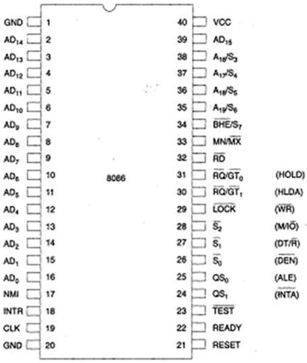
Let us now discuss the signals in detail −
Power supply and frequency signals
It uses 5V DC supply at VCC pin 40, and uses ground at VSS pin 1 and 20 for its operation.
Clock signal
Clock signal is provided through Pin-19. It provides timing to the processor for operations. Its frequency is different for different versions, i.e. 5MHz, 8MHz and 10MHz.
Address/data bus
AD0-AD15. These are 16 address/data bus. AD0-AD7 carries low order byte data and AD8AD15 carries higher order byte data. During the first clock cycle, it carries 16-bit address and after that it carries 16-bit data.
Address/status bus
A16-A19/S3-S6. These are the 4 address/status buses. During the first clock cycle, it carries 4-bit address and later it carries status signals.
S7/BHE
BHE stands for Bus High Enable. It is available at pin 34 and used to indicate the transfer of data using data bus D8-D15. This signal is low during the first clock cycle, thereafter it is active.
Read($\overline{RD}$)
It is available at pin 32 and is used to read signal for Read operation.
Ready
It is available at pin 32. It is an acknowledgement signal from I/O devices that data is transferred. It is an active high signal. When it is high, it indicates that the device is ready to transfer data. When it is low, it indicates wait state.
RESET
It is available at pin 21 and is used to restart the execution. It causes the processor to immediately terminate its present activity. This signal is active high for the first 4 clock cycles to RESET the microprocessor.
INTR
It is available at pin 18. It is an interrupt request signal, which is sampled during the last clock cycle of each instruction to determine if the processor considered this as an interrupt or not.
NMI
It stands for non-maskable interrupt and is available at pin 17. It is an edge triggered input, which causes an interrupt request to the microprocessor.
$\overline{TEST}$
This signal is like wait state and is available at pin 23. When this signal is high, then the processor has to wait for IDLE state, else the execution continues.
MN/$\overline{MX}$
It stands for Minimum/Maximum and is available at pin 33. It indicates what mode the processor is to operate in; when it is high, it works in the minimum mode and vice-aversa.
INTA
It is an interrupt acknowledgement signal and id available at pin 24. When the microprocessor receives this signal, it acknowledges the interrupt.
ALE
It stands for address enable latch and is available at pin 25. A positive pulse is generated each time the processor begins any operation. This signal indicates the availability of a valid address on the address/data lines.
DEN
It stands for Data Enable and is available at pin 26. It is used to enable Transreceiver 8286. The transreceiver is a device used to separate data from the address/data bus.
DT/R
It stands for Data Transmit/Receive signal and is available at pin 27. It decides the direction of data flow through the transreceiver. When it is high, data is transmitted out and vice-a-versa.
M/IO
This signal is used to distinguish between memory and I/O operations. When it is high, it indicates I/O operation and when it is low indicates the memory operation. It is available at pin 28.
WR
It stands for write signal and is available at pin 29. It is used to write the data into the memory or the output device depending on the status of M/IO signal.
HLDA
It stands for Hold Acknowledgement signal and is available at pin 30. This signal acknowledges the HOLD signal.
HOLD
This signal indicates to the processor that external devices are requesting to access the address/data buses. It is available at pin 31.
QS1 and QS0
These are queue status signals and are available at pin 24 and 25. These signals provide the status of instruction queue. Their conditions are shown in the following table −
| QS0 | QS1 | Status |
|---|---|---|
| 0 | 0 | No operation |
| 0 | 1 | First byte of opcode from the queue |
| 1 | 0 | Empty the queue |
| 1 | 1 | Subsequent byte from the queue |
S0, S1, S2
These are the status signals that provide the status of operation, which is used by the Bus Controller 8288 to generate memory & I/O control signals. These are available at pin 26, 27, and 28. Following is the table showing their status −
| S2 | S1 | S0 | Status |
|---|---|---|---|
| 0 | 0 | 0 | Interrupt acknowledgement |
| 0 | 0 | 1 | I/O Read |
| 0 | 1 | 0 | I/O Write |
| 0 | 1 | 1 | Halt |
| 1 | 0 | 0 | Opcode fetch |
| 1 | 0 | 1 | Memory read |
| 1 | 1 | 0 | Memory write |
| 1 | 1 | 1 | Passive |
LOCK
When this signal is active, it indicates to the other processors not to ask the CPU to leave the system bus. It is activated using the LOCK prefix on any instruction and is available at pin 29.
RQ/GT1 and RQ/GT0
These are the Request/Grant signals used by the other processors requesting the CPU to release the system bus. When the signal is received by CPU, then it sends acknowledgment. RQ/GT0 has a higher priority than RQ/GT1.
Microprocessor - 8086 Instruction Sets
The 8086 microprocessor supports 8 types of instructions −
- Data Transfer Instructions
- Arithmetic Instructions
- Bit Manipulation Instructions
- String Instructions
- Program Execution Transfer Instructions (Branch & Loop Instructions)
- Processor Control Instructions
- Iteration Control Instructions
- Interrupt Instructions
Let us now discuss these instruction sets in detail.
Data Transfer Instructions
These instructions are used to transfer the data from the source operand to the destination operand. Following are the list of instructions under this group −
Instruction to transfer a word
- MOV − Used to copy the byte or word from the provided source to the provided destination.
- PPUSH − Used to put a word at the top of the stack.
- POP − Used to get a word from the top of the stack to the provided location.
- PUSHA − Used to put all the registers into the stack.
- POPA − Used to get words from the stack to all registers.
- XCHG − Used to exchange the data from two locations.
- XLAT − Used to translate a byte in AL using a table in the memory.
Instructions for input and output port transfer
- IN − Used to read a byte or word from the provided port to the accumulator.
- OUT − Used to send out a byte or word from the accumulator to the provided port.
Instructions to transfer the address
- LEA − Used to load the address of operand into the provided register.
- LDS − Used to load DS register and other provided register from the memory
- LES − Used to load ES register and other provided register from the memory.
Instructions to transfer flag registers
- LAHF − Used to load AH with the low byte of the flag register.
- SAHF − Used to store AH register to low byte of the flag register.
- PUSHF − Used to copy the flag register at the top of the stack.
- POPF − Used to copy a word at the top of the stack to the flag register.
Arithmetic Instructions
These instructions are used to perform arithmetic operations like addition, subtraction, multiplication, division, etc.
Following is the list of instructions under this group −
Instructions to perform addition
- ADD − Used to add the provided byte to byte/word to word.
- ADC − Used to add with carry.
- INC − Used to increment the provided byte/word by 1.
- AAA − Used to adjust ASCII after addition.
- DAA − Used to adjust the decimal after the addition/subtraction operation.
Instructions to perform subtraction
- SUB − Used to subtract the byte from byte/word from word.
- SBB − Used to perform subtraction with borrow.
- DEC − Used to decrement the provided byte/word by 1.
- NPG − Used to negate each bit of the provided byte/word and add 1/2’s complement.
- CMP − Used to compare 2 provided byte/word.
- AAS − Used to adjust ASCII codes after subtraction.
- DAS − Used to adjust decimal after subtraction.
Instruction to perform multiplication
- MUL − Used to multiply unsigned byte by byte/word by word.
- IMUL − Used to multiply signed byte by byte/word by word.
- AAM − Used to adjust ASCII codes after multiplication.
Instructions to perform division
- DIV − Used to divide the unsigned word by byte or unsigned double word by word.
- IDIV − Used to divide the signed word by byte or signed double word by word.
- AAD − Used to adjust ASCII codes after division.
- CBW − Used to fill the upper byte of the word with the copies of sign bit of the lower byte.
- CWD − Used to fill the upper word of the double word with the sign bit of the lower word.
Bit Manipulation Instructions
These instructions are used to perform operations where data bits are involved, i.e. operations like logical, shift, etc.
Following is the list of instructions under this group −
Instructions to perform logical operation
- NOT − Used to invert each bit of a byte or word.
- AND − Used for adding each bit in a byte/word with the corresponding bit in another byte/word.
- OR − Used to multiply each bit in a byte/word with the corresponding bit in another byte/word.
- XOR − Used to perform Exclusive-OR operation over each bit in a byte/word with the corresponding bit in another byte/word.
- TEST − Used to add operands to update flags, without affecting operands.
Instructions to perform shift operations
- SHL/SAL − Used to shift bits of a byte/word towards left and put zero(S) in LSBs.
- SHR − Used to shift bits of a byte/word towards the right and put zero(S) in MSBs.
- SAR − Used to shift bits of a byte/word towards the right and copy the old MSB into the new MSB.
Instructions to perform rotate operations
- ROL − Used to rotate bits of byte/word towards the left, i.e. MSB to LSB and to Carry Flag [CF].
- ROR − Used to rotate bits of byte/word towards the right, i.e. LSB to MSB and to Carry Flag [CF].
- RCR − Used to rotate bits of byte/word towards the right, i.e. LSB to CF and CF to MSB.
- RCL − Used to rotate bits of byte/word towards the left, i.e. MSB to CF and CF to LSB.
String Instructions
String is a group of bytes/words and their memory is always allocated in a sequential order.
Following is the list of instructions under this group −
- REP − Used to repeat the given instruction till CX ≠ 0.
- REPE/REPZ − Used to repeat the given instruction until CX = 0 or zero flag ZF = 1.
- REPNE/REPNZ − Used to repeat the given instruction until CX = 0 or zero flag ZF = 1.
- MOVS/MOVSB/MOVSW − Used to move the byte/word from one string to another.
- COMS/COMPSB/COMPSW − Used to compare two string bytes/words.
- INS/INSB/INSW − Used as an input string/byte/word from the I/O port to the provided memory location.
- OUTS/OUTSB/OUTSW − Used as an output string/byte/word from the provided memory location to the I/O port.
- SCAS/SCASB/SCASW − Used to scan a string and compare its byte with a byte in AL or string word with a word in AX.
- LODS/LODSB/LODSW − Used to store the string byte into AL or string word into AX.
Program Execution Transfer Instructions (Branch and Loop Instructions)
These instructions are used to transfer/branch the instructions during an execution. It includes the following instructions −
Instructions to transfer the instruction during an execution without any condition −
- CALL − Used to call a procedure and save their return address to the stack.
- RET − Used to return from the procedure to the main program.
- JMP − Used to jump to the provided address to proceed to the next instruction.
Instructions to transfer the instruction during an execution with some conditions −
- JA/JNBE − Used to jump if above/not below/equal instruction satisfies.
- JAE/JNB − Used to jump if above/not below instruction satisfies.
- JBE/JNA − Used to jump if below/equal/ not above instruction satisfies.
- JC − Used to jump if carry flag CF = 1
- JE/JZ − Used to jump if equal/zero flag ZF = 1
- JG/JNLE − Used to jump if greater/not less than/equal instruction satisfies.
- JGE/JNL − Used to jump if greater than/equal/not less than instruction satisfies.
- JL/JNGE − Used to jump if less than/not greater than/equal instruction satisfies.
- JLE/JNG − Used to jump if less than/equal/if not greater than instruction satisfies.
- JNC − Used to jump if no carry flag (CF = 0)
- JNE/JNZ − Used to jump if not equal/zero flag ZF = 0
- JNO − Used to jump if no overflow flag OF = 0
- JNP/JPO − Used to jump if not parity/parity odd PF = 0
- JNS − Used to jump if not sign SF = 0
- JO − Used to jump if overflow flag OF = 1
- JP/JPE − Used to jump if parity/parity even PF = 1
- JS − Used to jump if sign flag SF = 1
Processor Control Instructions
These instructions are used to control the processor action by setting/resetting the flag values.
Following are the instructions under this group −
- STC − Used to set carry flag CF to 1
- CLC − Used to clear/reset carry flag CF to 0
- CMC − Used to put complement at the state of carry flag CF.
- STD − Used to set the direction flag DF to 1
- CLD − Used to clear/reset the direction flag DF to 0
- STI − Used to set the interrupt enable flag to 1, i.e., enable INTR input.
- CLI − Used to clear the interrupt enable flag to 0, i.e., disable INTR input.
Iteration Control Instructions
These instructions are used to execute the given instructions for number of times. Following is the list of instructions under this group −
- LOOP − Used to loop a group of instructions until the condition satisfies, i.e., CX = 0
- LOOPE/LOOPZ − Used to loop a group of instructions till it satisfies ZF = 1 & CX = 0
- LOOPNE/LOOPNZ − Used to loop a group of instructions till it satisfies ZF = 0 & CX = 0
- JCXZ − Used to jump to the provided address if CX = 0
Interrupt Instructions
These instructions are used to call the interrupt during program execution.
- INT − Used to interrupt the program during execution and calling service specified.
- INTO − Used to interrupt the program during execution if OF = 1
- IRET − Used to return from interrupt service to the main program
Microprocessor - 8086 Interrupts
Interrupt is the method of creating a temporary halt during program execution and allows peripheral devices to access the microprocessor. The microprocessor responds to that interrupt with an ISR (Interrupt Service Routine), which is a short program to instruct the microprocessor on how to handle the interrupt.
The following image shows the types of interrupts we have in a 8086 microprocessor −
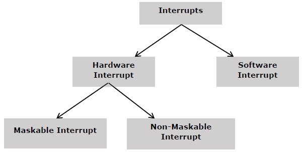
Hardware Interrupts
Hardware interrupt is caused by any peripheral device by sending a signal through a specified pin to the microprocessor.
The 8086 has two hardware interrupt pins, i.e. NMI and INTR. NMI is a non-maskable interrupt and INTR is a maskable interrupt having lower priority. One more interrupt pin associated is INTA called interrupt acknowledge.
NMI
It is a single non-maskable interrupt pin (NMI) having higher priority than the maskable interrupt request pin (INTR)and it is of type 2 interrupt.
When this interrupt is activated, these actions take place −
- Completes the current instruction that is in progress.
- Pushes the Flag register values on to the stack.
- Pushes the CS (code segment) value and IP (instruction pointer) value of the return address on to the stack.
- IP is loaded from the contents of the word location 00008H.
- CS is loaded from the contents of the next word location 0000AH.
- Interrupt flag and trap flag are reset to 0.
INTR
The INTR is a maskable interrupt because the microprocessor will be interrupted only if interrupts are enabled using set interrupt flag instruction. It should not be enabled using clear interrupt Flag instruction.
The INTR interrupt is activated by an I/O port. If the interrupt is enabled and NMI is disabled, then the microprocessor first completes the current execution and sends ‘0’ on INTA pin twice. The first ‘0’ means INTA informs the external device to get ready and during the second ‘0’ the microprocessor receives the 8 bit, say X, from the programmable interrupt controller.
These actions are taken by the microprocessor −
- First completes the current instruction.
- Activates INTA output and receives the interrupt type, say X.
- Flag register value, CS value of the return address and IP value of the return address are pushed on to the stack.
- IP value is loaded from the contents of word location X × 4
- CS is loaded from the contents of the next word location.
- Interrupt flag and trap flag is reset to 0
Software Interrupts
Some instructions are inserted at the desired position into the program to create interrupts. These interrupt instructions can be used to test the working of various interrupt handlers. It includes −
INT- Interrupt instruction with type number
It is 2-byte instruction. First byte provides the op-code and the second byte provides the interrupt type number. There are 256 interrupt types under this group.
Its execution includes the following steps −
- Flag register value is pushed on to the stack.
- CS value of the return address and IP value of the return address are pushed on to the stack.
- IP is loaded from the contents of the word location ‘type number’ × 4
- CS is loaded from the contents of the next word location.
- Interrupt Flag and Trap Flag are reset to 0
The starting address for type0 interrupt is 000000H, for type1 interrupt is 00004H similarly for type2 is 00008H and ……so on. The first five pointers are dedicated interrupt pointers. i.e. −
- TYPE 0 interrupt represents division by zero situation.
- TYPE 1 interrupt represents single-step execution during the debugging of a program.
- TYPE 2 interrupt represents non-maskable NMI interrupt.
- TYPE 3 interrupt represents break-point interrupt.
- TYPE 4 interrupt represents overflow interrupt.
The interrupts from Type 5 to Type 31 are reserved for other advanced microprocessors, and interrupts from 32 to Type 255 are available for hardware and software interrupts.
INT 3-Break Point Interrupt Instruction
It is a 1-byte instruction having op-code is CCH. These instructions are inserted into the program so that when the processor reaches there, then it stops the normal execution of program and follows the break-point procedure.
Its execution includes the following steps −
- Flag register value is pushed on to the stack.
- CS value of the return address and IP value of the return address are pushed on to the stack.
- IP is loaded from the contents of the word location 3×4 = 0000CH
- CS is loaded from the contents of the next word location.
- Interrupt Flag and Trap Flag are reset to 0
INTO - Interrupt on overflow instruction
It is a 1-byte instruction and their mnemonic INTO. The op-code for this instruction is CEH. As the name suggests it is a conditional interrupt instruction, i.e. it is active only when the overflow flag is set to 1 and branches to the interrupt handler whose interrupt type number is 4. If the overflow flag is reset then, the execution continues to the next instruction.
Its execution includes the following steps −
- Flag register values are pushed on to the stack.
- CS value of the return address and IP value of the return address are pushed on to the stack.
- IP is loaded from the contents of word location 4×4 = 00010H
- CS is loaded from the contents of the next word location.
- Interrupt flag and Trap flag are reset to 0
Microprocessor - 8086 Addressing Modes
The different ways in which a source operand is denoted in an instruction is known as addressing modes. There are 8 different addressing modes in 8086 programming −
Immediate addressing mode
The addressing mode in which the data operand is a part of the instruction itself is known as immediate addressing mode.
Example
MOV CX, 4929 H, ADD AX, 2387 H, MOV AL, FFH
Register addressing mode
It means that the register is the source of an operand for an instruction.
Example
MOV CX, AX   ; copies the contents of the 16-bit AX register into
             ; the 16-bit CX register),
ADD BX, AX
Direct addressing mode
The addressing mode in which the effective address of the memory location is written directly in the instruction.
Example
MOV AX, [1592H], MOV AL, [0300H]
Register indirect addressing mode
This addressing mode allows data to be addressed at any memory location through an offset address held in any of the following registers: BP, BX, DI & SI.
Example
MOV AX, [BX]  ; Suppose the register BX contains 4895H, then the contents
              ; 4895H are moved to AX
ADD CX, {BX}
Based addressing mode
In this addressing mode, the offset address of the operand is given by the sum of contents of the BX/BP registers and 8-bit/16-bit displacement.
Example
MOV DX, [BX+04], ADD CL, [BX+08]
Indexed addressing mode
In this addressing mode, the operands offset address is found by adding the contents of SI or DI register and 8-bit/16-bit displacements.
Example
MOV BX, [SI+16], ADD AL, [DI+16]
Based-index addressing mode
In this addressing mode, the offset address of the operand is computed by summing the base register to the contents of an Index register.
Example
ADD CX, [AX+SI], MOV AX, [AX+DI]
Based indexed with displacement mode
In this addressing mode, the operands offset is computed by adding the base register contents. An Index registers contents and 8 or 16-bit displacement.
Example
MOV AX, [BX+DI+08], ADD CX, [BX+SI+16]


No comments:
Post a Comment