Introduction:
A microprocessor is a controlling unit of a micro-computer, fabricated on a small chip capable of performing Arithmetic Logical Unit (ALU) operations and communicating with the other devices connected to it. In this tutorial, we will discuss the architecture, pin diagram and other key concepts of microprocessors.
8085 is pronounced as "eighty-eighty-five" microprocessor. It is an 8-bit microprocessor designed by Intel in 1977 using NMOS technology.
It has the following configuration −
- 8-bit data bus
- 16-bit address bus, which can address upto 64KB
- A 16-bit program counter
- A 16-bit stack pointer
- Six 8-bit registers arranged in pairs: BC, DE, HL
- Requires +5V supply to operate at 3.2 MHZ single phase clock
It is used in washing machines, microwave ovens, mobile phones, etc.
8085 Microprocessor – Functional Units
8085 consists of the following functional units −
Accumulator
It is an 8-bit register used to perform arithmetic, logical, I/O & LOAD/STORE operations. It is connected to internal data bus & ALU.
Arithmetic and logic unit
As the name suggests, it performs arithmetic and logical operations like Addition, Subtraction, AND, OR, etc. on 8-bit data.
General purpose register
There are 6 general purpose registers in 8085 processor, i.e. B, C, D, E, H & L. Each register can hold 8-bit data.
These registers can work in pair to hold 16-bit data and their pairing combination is like B-C, D-E & H-L.
Program counter
It is a 16-bit register used to store the memory address location of the next instruction to be executed. Microprocessor increments the program whenever an instruction is being executed, so that the program counter points to the memory address of the next instruction that is going to be executed.
Stack pointer
It is also a 16-bit register works like stack, which is always incremented/decremented by 2 during push & pop operations.
Temporary register
It is an 8-bit register, which holds the temporary data of arithmetic and logical operations.
Flag register
It is an 8-bit register having five 1-bit flip-flops, which holds either 0 or 1 depending upon the result stored in the accumulator.
These are the set of 5 flip-flops −
- Sign (S)
- Zero (Z)
- Auxiliary Carry (AC)
- Parity (P)
- Carry (C)
Its bit position is shown in the following table −
| D7 | D6 | D5 | D4 | D3 | D2 | D1 | D0 |
|---|---|---|---|---|---|---|---|
| S | Z | AC | P | CY |
Instruction register and decoder
It is an 8-bit register. When an instruction is fetched from memory then it is stored in the Instruction register. Instruction decoder decodes the information present in the Instruction register.
Timing and control unit
It provides timing and control signal to the microprocessor to perform operations. Following are the timing and control signals, which control external and internal circuits −
- Control Signals: READY, RD’, WR’, ALE
- Status Signals: S0, S1, IO/M’
- DMA Signals: HOLD, HLDA
- RESET Signals: RESET IN, RESET OUT
Interrupt control
As the name suggests it controls the interrupts during a process. When a microprocessor is executing a main program and whenever an interrupt occurs, the microprocessor shifts the control from the main program to process the incoming request. After the request is completed, the control goes back to the main program.
There are 5 interrupt signals in 8085 microprocessor: INTR, RST 7.5, RST 6.5, RST 5.5, TRAP.
Serial Input/output control
It controls the serial data communication by using these two instructions: SID (Serial input data) and SOD (Serial output data).
Address buffer and address-data buffer
The content stored in the stack pointer and program counter is loaded into the address buffer and address-data buffer to communicate with the CPU. The memory and I/O chips are connected to these buses; the CPU can exchange the desired data with the memory and I/O chips.
Address bus and data bus
Data bus carries the data to be stored. It is bidirectional, whereas address bus carries the location to where it should be stored and it is unidirectional. It is used to transfer the data & Address I/O devices.
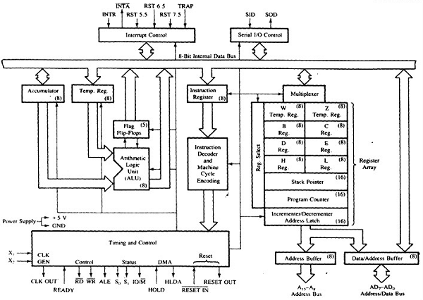
8085 Architecture
We have tried to depict the architecture of 8085 with this following image −
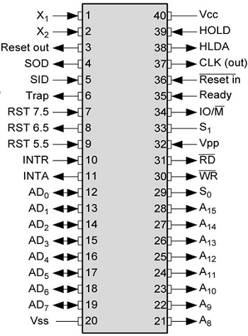
Microprocessor - 8085 Pin Configuration
The following image depicts the pin diagram of 8085 Microprocessor −
The pins of a 8085 microprocessor can be classified into seven groups −
Address bus
A15-A8, it carries the most significant 8-bits of memory/IO address.
Data bus
AD7-AD0, it carries the least significant 8-bit address and data bus.
Control and status signals
These signals are used to identify the nature of operation. There are 3 control signal and 3 status signals.
Three control signals are RD, WR & ALE.
- RD − This signal indicates that the selected IO or memory device is to be read and is ready for accepting data available on the data bus.
- WR − This signal indicates that the data on the data bus is to be written into a selected memory or IO location.
- ALE − It is a positive going pulse generated when a new operation is started by the microprocessor. When the pulse goes high, it indicates address. When the pulse goes down it indicates data.
Three status signals are IO/M, S0 & S1.
IO/M
This signal is used to differentiate between IO and Memory operations, i.e. when it is high indicates IO operation and when it is low then it indicates memory operation.
S1 & S0
These signals are used to identify the type of current operation.
Power supply
There are 2 power supply signals − VCC & VSS. VCC indicates +5v power supply and VSS indicates ground signal.
Clock signals
There are 3 clock signals, i.e. X1, X2, CLK OUT.
- X1, X2 − A crystal (RC, LC N/W) is connected at these two pins and is used to set frequency of the internal clock generator. This frequency is internally divided by 2.
- CLK OUT − This signal is used as the system clock for devices connected with the microprocessor.
Interrupts & externally initiated signals
Interrupts are the signals generated by external devices to request the microprocessor to perform a task. There are 5 interrupt signals, i.e. TRAP, RST 7.5, RST 6.5, RST 5.5, and INTR. We will discuss interrupts in detail in interrupts section.
- INTA − It is an interrupt acknowledgment signal.
- RESET IN − This signal is used to reset the microprocessor by setting the program counter to zero.
- RESET OUT − This signal is used to reset all the connected devices when the microprocessor is reset.
- READY − This signal indicates that the device is ready to send or receive data. If READY is low, then the CPU has to wait for READY to go high.
- HOLD − This signal indicates that another master is requesting the use of the address and data buses.
- HLDA (HOLD Acknowledge) − It indicates that the CPU has received the HOLD request and it will relinquish the bus in the next clock cycle. HLDA is set to low after the HOLD signal is removed.
Serial I/O signals
There are 2 serial signals, i.e. SID and SOD and these signals are used for serial communication.
- SOD (Serial output data line) − The output SOD is set/reset as specified by the SIM instruction.
- SID (Serial input data line) − The data on this line is loaded into accumulator whenever a RIM instruction is executed.
Now let us discuss the addressing modes in 8085 Microprocessor.
Addressing Modes in 8085
These are the instructions used to transfer the data from one register to another register, from the memory to the register, and from the register to the memory without any alteration in the content. Addressing modes in 8085 is classified into 5 groups −
Immediate addressing mode
In this mode, the 8/16-bit data is specified in the instruction itself as one of its operand. For example: MVI K, 20F: means 20F is copied into register K.
Register addressing mode
In this mode, the data is copied from one register to another. For example:MOV K, B: means data in register B is copied to register K.
Direct addressing mode
In this mode, the data is directly copied from the given address to the register. For example: LDB 5000K: means the data at address 5000K is copied to register B.
Indirect addressing mode
In this mode, the data is transferred from one register to another by using the address pointed by the register. For example: MOV K, B: means data is transferred from the memory address pointed by the register to the register K.
Implied addressing mode
This mode doesn’t require any operand; the data is specified by the opcode itself. For example: CMP.
Interrupts in 8085
Interrupts are the signals generated by the external devices to request the microprocessor to perform a task. There are 5 interrupt signals, i.e. TRAP, RST 7.5, RST 6.5, RST 5.5, and INTR.
Interrupt are classified into following groups based on their parameter −
- Vector interrupt − In this type of interrupt, the interrupt address is known to the processor. For example: RST7.5, RST6.5, RST5.5, TRAP.
- Non-Vector interrupt − In this type of interrupt, the interrupt address is not known to the processor so, the interrupt address needs to be sent externally by the device to perform interrupts. For example: INTR.
- Maskable interrupt − In this type of interrupt, we can disable the interrupt by writing some instructions into the program. For example:RST7.5, RST6.5, RST5.5.
- Non-Maskable interrupt − In this type of interrupt, we cannot disable the interrupt by writing some instructions into the program. For example: TRAP.
- Software interrupt − In this type of interrupt, the programmer has to add the instructions into the program to execute the interrupt. There are 8 software interrupts in 8085, i.e. RST0, RST1, RST2, RST3, RST4, RST5, RST6, and RST7.
- Hardware interrupt − There are 5 interrupt pins in 8085 used as hardware interrupts, i.e. TRAP, RST7.5, RST6.5, RST5.5, INTA.
Note − NTA is not an interrupt, it is used by the microprocessor for sending acknowledgement. TRAP has the highest priority, then RST7.5 and so on.
Interrupt Service Routine (ISR)
A small program or a routine that when executed, services the corresponding interrupting source is called an ISR.
TRAP
It is a non-maskable interrupt, having the highest priority among all interrupts. Bydefault, it is enabled until it gets acknowledged. In case of failure, it executes as ISR and sends the data to backup memory. This interrupt transfers the control to the location 0024H.
RST7.5
It is a maskable interrupt, having the second highest priority among all interrupts. When this interrupt is executed, the processor saves the content of the PC register into the stack and branches to 003CH address.
RST 6.5
It is a maskable interrupt, having the third highest priority among all interrupts. When this interrupt is executed, the processor saves the content of the PC register into the stack and branches to 0034H address.
RST 5.5
It is a maskable interrupt. When this interrupt is executed, the processor saves the content of the PC register into the stack and branches to 002CH address.
INTR
It is a maskable interrupt, having the lowest priority among all interrupts. It can be disabled by resetting the microprocessor.
When INTR signal goes high, the following events can occur −
- The microprocessor checks the status of INTR signal during the execution of each instruction.
- When the INTR signal is high, then the microprocessor completes its current instruction and sends active low interrupt acknowledge signal.
- When instructions are received, then the microprocessor saves the address of the next instruction on stack and executes the received instruction.
Microprocessor - 8085 Instruction Sets
Instruction sets are instruction codes to perform some task. It is classified into five categories.
| S.No. | Instruction & Description |
|---|---|
| 1 | Control Instructions
Following is the table showing the list of Control instructions with their meanings.
|
| 2 | Logical Instructions
Following is the table showing the list of Logical instructions with their meanings.
|
| 3 | Branching Instructions
Following is the table showing the list of Branching instructions with their meanings.
|
| 4 | Arithmetic Instructions
Following is the table showing the list of Arithmetic instructions with their meanings.
|
| 5 | Data Transfer Instructions
Following is the table showing the list of Data-transfer instructions with their meanings.
|
8085 – Demo Programs
Now, let us take a look at some program demonstrations using the above instructions −
Adding Two 8-bit Numbers
Write a program to add data at 3005H & 3006H memory location and store the result at 3007H memory location.
Problem demo −
(3005H) = 14H
   (3006H) = 89H
Result −
14H + 89H = 9DH
The program code can be written like this −
LXI H 3005H   : "HL points 3005H"
MOV A, M      : "Getting first operand"
INX H         : "HL points 3006H"
ADD M         : "Add second operand"
INX H         : "HL points 3007H"
MOV M, A      : "Store result at 3007H"
HLT           : "Exit program
Microprocessor - 8085 Control Instructions
Following is the table showing the list of Control instructions with their meanings.
| Opcode | Operand | Meaning | Explanation |
|---|---|---|---|
| NOP | None | No operation | No operation is performed, i.e., the instruction is fetched and decoded. |
| HLT | None | Halt and enter wait state | The CPU finishes executing the current instruction and stops further execution. An interrupt or reset is necessary to exit from the halt state. |
| DI | None | Disable interrupts | The interrupt enable flip-flop is reset and all the interrupts are disabled except TRAP. |
| EI | None | Enable interrupts | The interrupt enable flip-flop is set and all the interrupts are enabled. |
| RIM | None | Read interrupt mask | This instruction is used to read the status of interrupts 7.5, 6.5, 5.5 and read serial data input bit. |
| SIM | None | Set interrupt mask | This instruction is used to implement the interrupts 7.5, 6.5, 5.5, and serial data output. |
Microprocessor - 8085 Logical Instructions
The following table shows the list of Logical instructions with their meanings.
| Opcode | Operand | Meaning | Explanation |
|---|---|---|---|
| CMP |
R
M
| Compare the register or memory with the accumulator | The contents of the operand (register or memory) are M compared with the contents of the accumulator. |
| CPI | 8-bit data | Compare immediate with the accumulator | The second byte data is compared with the contents of the accumulator. |
| ANA |
R
M
| Logical AND register or memory with the accumulator | The contents of the accumulator are logically AND with M the contents of the register or memory, and the result is placed in the accumulator. |
| ANI | 8-bit data | Logical AND immediate with the accumulator | The contents of the accumulator are logically AND with the 8-bit data and the result is placed in the accumulator. |
| XRA |
R
M
| Exclusive OR register or memory with the accumulator | The contents of the accumulator are Exclusive OR with M the contents of the register or memory, and the result is placed in the accumulator. |
| XRI | 8-bit data | Exclusive OR immediate with the accumulator | The contents of the accumulator are Exclusive OR with the 8-bit data and the result is placed in the accumulator. |
| ORA |
R
M
| Logical OR register or memory with the accumulator | The contents of the accumulator are logically OR with M the contents of the register or memory, and result is placed in the accumulator. |
| ORI | 8-bit data | Logical OR immediate with the accumulator | The contents of the accumulator are logically OR with the 8-bit data and the result is placed in the accumulator. |
| RLC | None | Rotate the accumulator left | Each binary bit of the accumulator is rotated left by one position. Bit D7 is placed in the position of D0 as well as in the Carry flag. CY is modified according to bit D7. |
| RRC | None | Rotate the accumulator right | Each binary bit of the accumulator is rotated right by one position. Bit D0 is placed in the position of D7 as well as in the Carry flag. CY is modified according to bit D0. |
| RAL | None | Rotate the accumulator left through carry | Each binary bit of the accumulator is rotated left by one position through the Carry flag. Bit D7 is placed in the Carry flag, and the Carry flag is placed in the least significant position D0. CY is modified according to bit D7. |
| RAR | None | Rotate the accumulator right through carry | Each binary bit of the accumulator is rotated right by one position through the Carry flag. Bit D0 is placed in the Carry flag, and the Carry flag is placed in the most significant position D7. CY is modified according to bit D0. |
| CMA | None | Complement accumulator | The contents of the accumulator are complemented. No flags are affected. |
| CMC | None | Complement carry | The Carry flag is complemented. No other flags are affected. |
| STC | None | Set Carry | Set Carry |
8085 Arithmetic Instructions
Following is the table showing the list of Arithmetic instructions with their meanings.
| Opcode | Operand | Meaning | Explanation |
|---|---|---|---|
ADD
|
R
M
|
Add register or memory, to the accumulator
|
The contents of the register or memory are added to the contents of the accumulator and the result is stored in the accumulator.
Example − ADD K.
|
ADC
|
R
M
|
Add register to the accumulator with carry
|
The contents of the register or memory & M the Carry flag are added to the contents of the accumulator and the result is stored in the accumulator.
Example − ADC K
|
ADI
|
8-bit data
|
Add the immediate to the accumulator
|
The 8-bit data is added to the contents of the accumulator and the result is stored in the accumulator.
Example − ADI 55K
|
ACI
|
8-bit data
|
Add the immediate to the accumulator with carry
|
The 8-bit data and the Carry flag are added to the contents of the accumulator and the result is stored in the accumulator.
Example − ACI 55K
|
LXI
|
Reg. pair, 16bit data
|
Load the register pair immediate
|
The instruction stores 16-bit data into the register pair designated in the operand.
Example − LXI K, 3025M
|
DAD
|
Reg. pair
|
Add the register pair to H and L registers
|
The 16-bit data of the specified register pair are added to the contents of the HL register.
Example − DAD K
|
SUB
|
R
M
|
Subtract the register or the memory from the accumulator
|
The contents of the register or the memory are subtracted from the contents of the accumulator, and the result is stored in the accumulator.
Example − SUB K
|
SBB
|
R
M
|
Subtract the source and borrow from the accumulator
|
The contents of the register or the memory & M the Borrow flag are subtracted from the contents of the accumulator and the result is placed in the accumulator.
Example − SBB K
|
SUI
|
8-bit data
|
Subtract the immediate from the accumulator
|
The 8-bit data is subtracted from the contents of the accumulator & the result is stored in the accumulator.
Example − SUI 55K
|
SBI
|
8-bit data
|
Subtract the immediate from the accumulator with borrow
|
The contents of register H are exchanged with the contents of register D, and the contents of register L are exchanged with the contents of register E.
Example − XCHG
|
INR
|
R
M
|
Increment the register or the memory by 1
|
The contents of the designated register or the memory are incremented by 1 and their result is stored at the same place.
Example − INR K
|
INX
|
R
|
Increment register pair by 1
|
The contents of the designated register pair are incremented by 1 and their result is stored at the same place.
Example − INX K
|
DCR
|
R
M
|
Decrement the register or the memory by 1
|
The contents of the designated register or memory are decremented by 1 and their result is stored at the same place.
Example − DCR K
|
DCX
|
R
|
Decrement the register pair by 1
|
The contents of the designated register pair are decremented by 1 and their result is stored at the same place.
Example − DCX K
|
DAA
|
None
|
Decimal adjust accumulator
|
The contents of the accumulator are changed from a binary value to two 4-bit BCD digits.
If the value of the low-order 4-bits in the accumulator is greater than 9 or if AC flag is set, the instruction adds 6 to the low-order four bits.
If the value of the high-order 4-bits in the accumulator is greater than 9 or if the Carry flag is set, the instruction adds 6 to the high-order four bits.
Example − DAA
|
8085 Data-transfer Instructions
Following is the table showing the list of Data-transfer instructions with their meanings.
| Opcode | Operand | Meaning | Explanation |
|---|---|---|---|
| MOV |
Rd, Sc
M, Sc
Dt, M
|
Copy from the source (Sc) to the destination(Dt)
|
This instruction copies the contents of the source register into the destination register without any alteration.
Example − MOV K, L
|
MVI
|
Rd, data
M, data
|
Move immediate 8-bit
|
The 8-bit data is stored in the destination register or memory.
Example − MVI K, 55L
|
LDA
|
16-bit address
|
Load the accumulator
|
The contents of a memory location, specified by a 16-bit address in the operand, are copied to the accumulator.
Example − LDA 2034K
|
LDAX
|
B/D Reg. pair
|
Load the accumulator indirect
|
The contents of the designated register pair point to a memory location. This instruction copies the contents of that memory location into the accumulator.
Example − LDAX K
|
LXI
|
Reg. pair, 16-bit data
|
Load the register pair immediate
|
The instruction loads 16-bit data in the register pair designated in the register or the memory.
Example − LXI K, 3225L
|
LHLD
|
16-bit address
|
Load H and L registers direct
|
The instruction copies the contents of the memory location pointed out by the address into register L and copies the contents of the next memory location into register H.
Example − LHLD 3225K
|
STA
|
16-bit address
|
16-bit address
|
The contents of the accumulator are copied into the memory location specified by the operand.
This is a 3-byte instruction, the second byte specifies the low-order address and the third byte specifies the high-order address.
Example − STA 325K
|
STAX
|
16-bit address
|
Store the accumulator indirect
|
The contents of the accumulator are copied into the memory location specified by the contents of the operand.
Example − STAX K
|
SHLD
|
16-bit address
|
The contents of register L are stored in the memory location specified by the 16-bit address in the operand and the contents of H register are stored into the next memory location by incrementing the operand.
This is a 3-byte instruction, the second byte specifies the low-order address and the third byte specifies the high-order address.
Example − SHLD 3225K
| |
XCHG
|
None
|
Exchange H and L with D and E
|
The contents of register H are exchanged with the contents of register D, and the contents of register L are exchanged with the contents of register E.
Example − XCHG
|
SPHL
|
None
|
Copy H and L registers to the stack pointer
|
The instruction loads the contents of the H and L registers into the stack pointer register. The contents of the H register provide the high-order address and the contents of the L register provide the low-order address.
Example − SPHL
|
XTHL
|
None
|
Exchange H and L with top of stack
|
The contents of the L register are exchanged with the stack location pointed out by the contents of the stack pointer register.
The contents of the H register are exchanged with the next stack location (SP+1).
Example − XTHL
|
PUSH
|
Reg. pair
|
Push the register pair onto the stack
|
The contents of the register pair designated in the operand are copied onto the stack in the following sequence.
The stack pointer register is decremented and the contents of the high order register (B, D, H, A) are copied into that location.
The stack pointer register is decremented again and the contents of the low-order register (C, E, L, flags) are copied to that location.
Example − PUSH K
|
POP
|
Reg. pair
|
Pop off stack to the register pair
|
The contents of the memory location pointed out by the stack pointer register are copied to the low-order register (C, E, L, status flags) of the operand.
The stack pointer is incremented by 1 and the contents of that memory location are copied to the high-order register (B, D, H, A) of the operand.
The stack pointer register is again incremented by 1.
Example − POPK
|
OUT
|
8-bit port address
|
Output the data from the accumulator to a port with 8bit address
|
The contents of the accumulator are copied into the I/O port specified by the operand.
Example − OUT K9L
|
IN
|
8-bit port address
|
Input data to accumulator from a port with 8-bit address
|
The contents of the input port designated in the operand are read and loaded into the accumulator.
Example − IN5KL
|


No comments:
Post a Comment