Friday 22 February 2019

UNIT - IV Peripheral Devices and I/O Interfacing

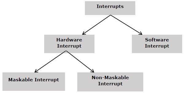
8259 PIC Microprocessor:

8259 microprocessor is defined as Programmable Interrupt Controller (PIC)microprocessor. There are 5 hardware interrupts and 2 hardware interrupts in 8085 and 8086 respectively. But by connecting 8259 with CPU, we can increase the interrupt handling capability. 8259 combines the multi interrupt input sources into a single interrupt output. Interfacing of single PIC provides 8 interrupts inputs from IR0-IR7.
For example, Interfacing of 8085 and 8259 increases the interrupt handling capability of 8085 microprocessor from 5 to 8 interrupt levels.
Features of 8259 PIC microprocessor –


  1. Intel 8259 is designed for Intel 8085 and Intel 8086 microprocessor.
  2. It can be programmed either in level triggered or in edge triggered interrupt level.
  3. We can masked individual bits of interrupt request register.
  4. We can increase interrupt handling capability upto 64 interrupt level by cascading further 8259 PIC.
  5. Clock cycle is not required.
Pin Diagram of 8259 –
We can see through above diagram that there are total 28 pins in 8259 PIC microprocessor where Vcc :5V Power supply and Gnd: ground. Other pins use are explained below.
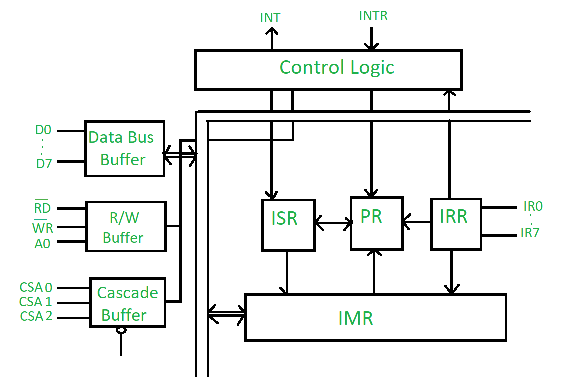
Block Diagram of 8259 PIC microprocessor –


The Block Diagram consists of 8 blocks which are – Data Bus Buffer, Read/Write Logic, Cascade Buffer Comparator, Control Logic, Priority Resolver and 3 registers- ISR, IRR, IMR.
  1. Data bus buffer –
    This Block is used as a mediator between 8259 and 8085/8086 microprocessor by acting as a buffer. It takes the control word from the 8085 (let say) microprocessor and transfer it to the control logic of 8259 microprocessor. Also, after selection of Interrupt by 8259 microprocessor, it transfer the opcode of the selected Interrupt and address of the Interrupt service sub routine to the other connected microprocessor. The data bus buffer consists of 8 bits represented as D0-D7 in the block diagram. Thus, shows that a maximum of 8 bits data can be transferred at a time.
  2. Read/Write logic –
    This block works only when the value of pin CS is low (as this pin is active low). This block is responsible for the flow of data depending upon the inputs of RD and WR. These two pins are active low pins used for read and write operations.
  3. Control logic –
    It is the centre of the microprocessor and controls the functioning of every block. It has pin INTR which is connected with other microprocessor for taking interrupt request and pin INT for giving the output. If 8259 is enabled, and the other microprocessor Interrupt flag is high then this causes the value of the output INT pin high and in this way 8259 responds to the request made by other microprocessor.
  4. Interrupt request register (IRR) –
    It stores all the interrupt level which are requesting for Interrupt services.
  5. Interrupt service register (ISR) –
    It stores the interrupt level which are currently being executed.
  6. Interrupt mask register (IMR) –
    It stores the interrupt level which have to be masked by storing the masking bits of the interrupt level.
  7. Priority resolver –
    It examines all the three registers and set the priority of interrupts and according to the priority of the interrupts, interrupt with highest priority is set in ISR register. Also, it reset the interrupt level which is already been serviced in IRR.
  8. Cascade buffer –
    To increase the Interrupt handling capability, we can further cascade more number of pins by using cascade buffer. So, during increment of interrupt capability, CSA lines are used to control multiple interrupt structure.
SP/EN (Slave program/Enable buffer) pin is when set to high, works in master mode else in slave mode. In Non Buffered mode, SP/EN pin is used to specify whether 8259 work as master or slave and in Buffered mode, SP/EN pin is used as an output to enable data bus.

Block Diagram of 8259 Microprocessor:

  • 8259 microprocessor can be programmed according to given interrupts condition and it can be provided either with level or edge triggered interrupt level.
  • It can be programmed either work in 8085 or in 8086 microprocessors.
  • Individual interrupt bits can be masked.
  • By conducting more number of 8259 we can get upto 64 interrupt pins.
It contains 3 rigisters commonly known as ISR, IRR, IMR & there is 1 priority resolver (PR).
  1. Interrupt Request Register (IRR): It stores those bits which are requesting for their interrupt services.
  2. Interrupt Service Register (ISR): It stores that interrupt levels which is currently being servied.
  3. Interrupt Mask Register (IMR): It stores that interrupt levels which have to be masked. These interrupts levels are already acccepted by 8259 microprocessor.
Priority Resolver (PR): It examines all the 3 registers and set the priority of interrupts and set the interrupt levels in ISR which has highest priority and rest the interrupt bit is IRR which is already accepted.
SP/EN (low active pin): If its value is 1 it works in master mode & if its value=e is 0 then it works in slave mode.
Cascade Buffer: It is used to cascade more number of Programmable Interrupt Controller to increase the interrupts handling capability upto 64 level.

8279 - Programmable Keyboard

8279 programmable keyboard/display controller is designed by Intel that interfaces a keyboard with the CPU. The keyboard first scans the keyboard and identifies if any key has been pressed. It then sends their relative response of the pressed key to the CPU and vice-a-versa.

How Many Ways the Keyboard is Interfaced with the CPU?

The Keyboard can be interfaced either in the interrupt or the polled mode. In the Interrupt mode, the processor is requested service only if any key is pressed, otherwise the CPU will continue with its main task.
In the Polled mode, the CPU periodically reads an internal flag of 8279 to check whether any key is pressed or not with key pressure.

How Does 8279 Keyboard Work?

The keyboard consists of maximum 64 keys, which are interfaced with the CPU by using the key-codes. These key-codes are de-bounced and stored in an 8-byte FIFORAM, which can be accessed by the CPU. If more than 8 characters are entered in the FIFO, then it means more than eight keys are pressed at a time. This is when the overrun status is set.
If a FIFO contains a valid key entry, then the CPU is interrupted in an interrupt mode else the CPU checks the status in polling to read the entry. Once the CPU reads a key entry, then FIFO is updated, and the key entry is pushed out of the FIFO to generate space for new entries.

Architecture and Description

8279 Architecture

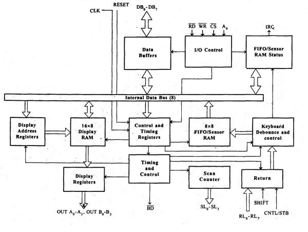
I/O Control and Data Buffer

This unit controls the flow of data through the microprocessor. It is enabled only when D is low. Its data buffer interfaces the external bus of the system with the internal bus of the microprocessor. The pins A0, RD, and WR are used for command, status or data read/write operations.

Control and Timing Register and Timing Control

This unit contains registers to store the keyboard, display modes, and other operations as programmed by the CPU. The timing and control unit handles the timings for the operation of the circuit.

Scan Counter

It has two modes i.e. Encoded mode and Decoded mode. In the encoded mode, the counter provides the binary count that is to be externally decoded to provide the scan lines for the keyboard and display.
In the decoded scan mode, the counter internally decodes the least significant 2 bits and provides a decoded 1 out of 4 scan on SL0-SL3.

Return Buffers, Keyboard Debounce, and Control

This unit first scans the key closure row-wise, if found then the keyboard debounce unit debounces the key entry. In case, the same key is detected, then the code of that key is directly transferred to the sensor RAM along with SHIFT & CONTROL key status.

FIFO/Sensor RAM and Status Logic

This unit acts as 8-byte first-in-first-out (FIFO) RAM where the key code of every pressed key is entered into the RAM as per their sequence. The status logic generates an interrupt request after each FIFO read operation till the FIFO gets empty.
In the scanned sensor matrix mode, this unit acts as sensor RAM where its each row is loaded with the status of their corresponding row of sensors into the matrix. When the sensor changes its state, the IRQ line changes to high and interrupts the CPU.

Display Address Registers and Display RAM

This unit consists of display address registers which holds the addresses of the word currently read/written by the CPU to/from the display RAM.

8279 − Pin Description

The following figure shows the pin diagram of 8279 −
8279 Pin Diagram

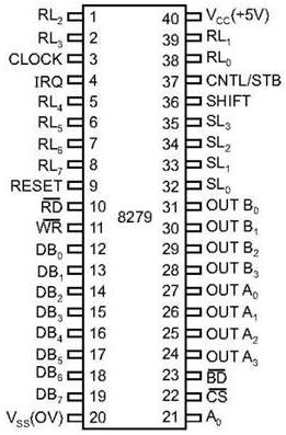
Data Bus Lines, DB0 - DB7

These are 8 bidirectional data bus lines used to transfer the data to/from the CPU.

CLK

The clock input is used to generate internal timings required by the microprocessor.

RESET

As the name suggests this pin is used to reset the microprocessor.

CS Chip Select

When this pin is set to low, it allows read/write operations, else this pin should be set to high.

A0

This pin indicates the transfer of command/status information. When it is low, it indicates the transfer of data.

RD, WR

This Read/Write pin enables the data buffer to send/receive data over the data bus.

IRQ

This interrupt output line goes high when there is data in the FIFO sensor RAM. The interrupt line goes low with each FIFO RAM read operation. However, if the FIFO RAM further contains any key-code entry to be read by the CPU, this pin again goes high to generate an interrupt to the CPU.

Vss, Vcc

These are the ground and power supply lines of the microprocessor.

SL0 − SL3

These are the scan lines used to scan the keyboard matrix and display the digits. These lines can be programmed as encoded or decoded, using the mode control register.

RL0 − RL7

These are the Return Lines which are connected to one terminal of keys, while the other terminal of the keys is connected to the decoded scan lines. These lines are set to 0 when any key is pressed.

SHIFT

The Shift input line status is stored along with every key code in FIFO in the scanned keyboard mode. Till it is pulled low with a key closure, it is pulled up internally to keep it high

CNTL/STB - CONTROL/STROBED I/P Mode

In the keyboard mode, this line is used as a control input and stored in FIFO on a key closure. The line is a strobe line that enters the data into FIFO RAM, in the strobed input mode. It has an internal pull up. The line is pulled down with a key closure.

BD

It stands for blank display. It is used to blank the display during digit switching.

OUTA0 – OUTA3 and OUTB0 – OUTB3

These are the output ports for two 16x4 or one 16x8 internal display refresh registers. The data from these lines is synchronized with the scan lines to scan the display and the keyboard.

Operational Modes of 8279

There are two modes of operation on 8279 − Input Mode and Output Mode.

Input Mode

This mode deals with the input given by the keyboard and this mode is further classified into 3 modes.
  • Scanned Keyboard Mode − In this mode, the key matrix can be interfaced using either encoded or decoded scans. In the encoded scan, an 8×8 keyboard or in the decoded scan, a 4×8 keyboard can be interfaced. The code of key pressed with SHIFT and CONTROL status is stored into the FIFO RAM.
  • Scanned Sensor Matrix − In this mode, a sensor array can be interfaced with the processor using either encoder or decoder scans. In the encoder scan, 8×8 sensor matrix or with decoder scan 4×8 sensor matrix can be interfaced.
  • Strobed Input − In this mode, when the control line is set to 0, the data on the return lines is stored in the FIFO byte by byte.

Output Mode

This mode deals with display-related operations. This mode is further classified into two output modes.
  • Display Scan − This mode allows 8/16 character multiplexed displays to be organized as dual 4-bit/single 8-bit display units.
  • Display Entry − This mode allows the data to be entered for display either from the right side/left side.
  • Microprocessor - 8257 DMA Controller

DMA stands for Direct Memory Access. It is designed by Intel to transfer data at the fastest rate. It allows the device to transfer the data directly to/from memory without any interference of the CPU.
Using a DMA controller, the device requests the CPU to hold its data, address and control bus, so the device is free to transfer data directly to/from the memory. The DMA data transfer is initiated only after receiving HLDA signal from the CPU.

How DMA Operations are Performed?

Following is the sequence of operations performed by a DMA −
  • Initially, when any device has to send data between the device and the memory, the device has to send DMA request (DRQ) to DMA controller.
  • The DMA controller sends Hold request (HRQ) to the CPU and waits for the CPU to assert the HLDA.
  • Then the microprocessor tri-states all the data bus, address bus, and control bus. The CPU leaves the control over bus and acknowledges the HOLD request through HLDA signal.
  • Now the CPU is in HOLD state and the DMA controller has to manage the operations over buses between the CPU, memory, and I/O devices.

Features of 8257

Here is a list of some of the prominent features of 8257 −
  • It has four channels which can be used over four I/O devices.
  • Each channel has 16-bit address and 14-bit counter.
  • Each channel can transfer data up to 64kb.
  • Each channel can be programmed independently.
  • Each channel can perform read transfer, write transfer and verify transfer operations.
  • It generates MARK signal to the peripheral device that 128 bytes have been transferred.
  • It requires a single phase clock.
  • Its frequency ranges from 250Hz to 3MHz.
  • It operates in 2 modes, i.e., Master mode and Slave mode.
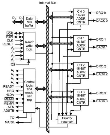
8257 Architecture

The following image shows the architecture of 8257 −
8257 Architecture

8257 Pin Description

The following image shows the pin diagram of a 8257 DMA controller −
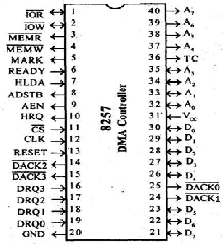
8257 Pin Diagram

DRQ0−DRQ3

These are the four individual channel DMA request inputs, which are used by the peripheral devices for using DMA services. When the fixed priority mode is selected, then DRQ0 has the highest priority and DRQ3 has the lowest priority among them.

DACKo − DACK3

These are the active-low DMA acknowledge lines, which updates the requesting peripheral about the status of their request by the CPU. These lines can also act as strobe lines for the requesting devices.

Do − D7

These are bidirectional, data lines which are used to interface the system bus with the internal data bus of DMA controller. In the Slave mode, it carries command words to 8257 and status word from 8257. In the master mode, these lines are used to send higher byte of the generated address to the latch. This address is further latched using ADSTB signal.

IOR

It is an active-low bidirectional tri-state input line, which is used by the CPU to read internal registers of 8257 in the Slave mode. In the master mode, it is used to read data from the peripheral devices during a memory write cycle.

IOW

It is an active low bi-direction tri-state line, which is used to load the contents of the data bus to the 8-bit mode register or upper/lower byte of a 16-bit DMA address register or terminal count register. In the master mode, it is used to load the data to the peripheral devices during DMA memory read cycle.

CLK

It is a clock frequency signal which is required for the internal operation of 8257.

RESET

This signal is used to RESET the DMA controller by disabling all the DMA channels.

Ao - A3

These are the four least significant address lines. In the slave mode, they act as an input, which selects one of the registers to be read or written. In the master mode, they are the four least significant memory address output lines generated by 8257.

CS

It is an active-low chip select line. In the Slave mode, it enables the read/write operations to/from 8257. In the master mode, it disables the read/write operations to/from 8257.

A4 - A7

These are the higher nibble of the lower byte address generated by DMA in the master mode.

READY

It is an active-high asynchronous input signal, which makes DMA ready by inserting wait states.

HRQ

This signal is used to receive the hold request signal from the output device. In the slave mode, it is connected with a DRQ input line 8257. In Master mode, it is connected with HOLD input of the CPU.

HLDA

It is the hold acknowledgement signal which indicates the DMA controller that the bus has been granted to the requesting peripheral by the CPU when it is set to 1.

MEMR

It is the low memory read signal, which is used to read the data from the addressed memory locations during DMA read cycles.

MEMW

It is the active-low three state signal which is used to write the data to the addressed memory location during DMA write operation.

ADST

This signal is used to convert the higher byte of the memory address generated by the DMA controller into the latches.

AEN

This signal is used to disable the address bus/data bus.

TC

It stands for ‘Terminal Count’, which indicates the present DMA cycle to the present peripheral devices.

MARK

The mark will be activated after each 128 cycles or integral multiples of it from the beginning. It indicates the current DMA cycle is the 128th cycle since the previous MARK output to the selected peripheral device.

Vcc

It is the power signal which is required for the operation of the circuit.

Friday 15 February 2019

UNIT - 3 8086 System Design

Microprocessor - 8086 Interrupts


Interrupt is the method of creating a temporary halt during program execution and allows peripheral devices to access the microprocessor. The microprocessor responds to that interrupt with an ISR (Interrupt Service Routine), which is a short program to instruct the microprocessor on how to handle the interrupt.
The following image shows the types of interrupts we have in a 8086 microprocessor −
Interrupts

Hardware Interrupts

Hardware interrupt is caused by any peripheral device by sending a signal through a specified pin to the microprocessor.
The 8086 has two hardware interrupt pins, i.e. NMI and INTR. NMI is a non-maskable interrupt and INTR is a maskable interrupt having lower priority. One more interrupt pin associated is INTA called interrupt acknowledge.

NMI

It is a single non-maskable interrupt pin (NMI) having higher priority than the maskable interrupt request pin (INTR)and it is of type 2 interrupt.
When this interrupt is activated, these actions take place −
  • Completes the current instruction that is in progress.
  • Pushes the Flag register values on to the stack.
  • Pushes the CS (code segment) value and IP (instruction pointer) value of the return address on to the stack.
  • IP is loaded from the contents of the word location 00008H.
  • CS is loaded from the contents of the next word location 0000AH.
  • Interrupt flag and trap flag are reset to 0.

INTR

The INTR is a maskable interrupt because the microprocessor will be interrupted only if interrupts are enabled using set interrupt flag instruction. It should not be enabled using clear interrupt Flag instruction.
The INTR interrupt is activated by an I/O port. If the interrupt is enabled and NMI is disabled, then the microprocessor first completes the current execution and sends ‘0’ on INTA pin twice. The first ‘0’ means INTA informs the external device to get ready and during the second ‘0’ the microprocessor receives the 8 bit, say X, from the programmable interrupt controller.
These actions are taken by the microprocessor −
  • First completes the current instruction.
  • Activates INTA output and receives the interrupt type, say X.
  • Flag register value, CS value of the return address and IP value of the return address are pushed on to the stack.
  • IP value is loaded from the contents of word location X × 4
  • CS is loaded from the contents of the next word location.
  • Interrupt flag and trap flag is reset to 0

Software Interrupts

Some instructions are inserted at the desired position into the program to create interrupts. These interrupt instructions can be used to test the working of various interrupt handlers. It includes −

INT- Interrupt instruction with type number

It is 2-byte instruction. First byte provides the op-code and the second byte provides the interrupt type number. There are 256 interrupt types under this group.
Its execution includes the following steps −
  • Flag register value is pushed on to the stack.
  • CS value of the return address and IP value of the return address are pushed on to the stack.
  • IP is loaded from the contents of the word location ‘type number’ × 4
  • CS is loaded from the contents of the next word location.
  • Interrupt Flag and Trap Flag are reset to 0
The starting address for type0 interrupt is 000000H, for type1 interrupt is 00004H similarly for type2 is 00008H and ……so on. The first five pointers are dedicated interrupt pointers. i.e. −
  • TYPE 0 interrupt represents division by zero situation.
  • TYPE 1 interrupt represents single-step execution during the debugging of a program.
  • TYPE 2 interrupt represents non-maskable NMI interrupt.
  • TYPE 3 interrupt represents break-point interrupt.
  • TYPE 4 interrupt represents overflow interrupt.
The interrupts from Type 5 to Type 31 are reserved for other advanced microprocessors, and interrupts from 32 to Type 255 are available for hardware and software interrupts.

INT 3-Break Point Interrupt Instruction

It is a 1-byte instruction having op-code is CCH. These instructions are inserted into the program so that when the processor reaches there, then it stops the normal execution of program and follows the break-point procedure.
Its execution includes the following steps −
  • Flag register value is pushed on to the stack.
  • CS value of the return address and IP value of the return address are pushed on to the stack.
  • IP is loaded from the contents of the word location 3×4 = 0000CH
  • CS is loaded from the contents of the next word location.
  • Interrupt Flag and Trap Flag are reset to 0

INTO - Interrupt on overflow instruction

It is a 1-byte instruction and their mnemonic INTO. The op-code for this instruction is CEH. As the name suggests it is a conditional interrupt instruction, i.e. it is active only when the overflow flag is set to 1 and branches to the interrupt handler whose interrupt type number is 4. If the overflow flag is reset then, the execution continues to the next instruction.
Its execution includes the following steps −
  • Flag register values are pushed on to the stack.
  • CS value of the return address and IP value of the return address are pushed on to the stack.
  • IP is loaded from the contents of word location 4×4 = 00010H
  • CS is loaded from the contents of the next word location.
  • Interrupt flag and Trap flag are reset to 0

Assembly Programming Tutorial


Assembly language is a low-level programming language for a computer or other programmable device specific to a particular computer architecture in contrast to most high-level programming languages, which are generally portable across multiple systems. Assembly language is converted into executable machine code by a utility program referred to as an assembler like NASM, MASM, etc.

What is Assembly Language?

Each personal computer has a microprocessor that manages the computer's arithmetical, logical, and control activities.
Each family of processors has its own set of instructions for handling various operations such as getting input from keyboard, displaying information on screen and performing various other jobs. These set of instructions are called 'machine language instructions'.
A processor understands only machine language instructions, which are strings of 1's and 0's. However, machine language is too obscure and complex for using in software development. So, the low-level assembly language is designed for a specific family of processors that represents various instructions in symbolic code and a more understandable form.

Advantages of Assembly Language

Having an understanding of assembly language makes one aware of −
  • How programs interface with OS, processor, and BIOS;
  • How data is represented in memory and other external devices;
  • How the processor accesses and executes instruction;
  • How instructions access and process data;
  • How a program accesses external devices.
Other advantages of using assembly language are −
  • It requires less memory and execution time;
  • It allows hardware-specific complex jobs in an easier way;
  • It is suitable for time-critical jobs;
  • It is most suitable for writing interrupt service routines and other memory resident programs.

Basic Features of PC Hardware

The main internal hardware of a PC consists of processor, memory, and registers. Registers are processor components that hold data and address. To execute a program, the system copies it from the external device into the internal memory. The processor executes the program instructions.
The fundamental unit of computer storage is a bit; it could be ON (1) or OFF (0). A group of nine related bits makes a byte, out of which eight bits are used for data and the last one is used for parity. According to the rule of parity, the number of bits that are ON (1) in each byte should always be odd.
So, the parity bit is used to make the number of bits in a byte odd. If the parity is even, the system assumes that there had been a parity error (though rare), which might have been caused due to hardware fault or electrical disturbance.
The processor supports the following data sizes −
  • Word: a 2-byte data item
  • Doubleword: a 4-byte (32 bit) data item
  • Quadword: an 8-byte (64 bit) data item
  • Paragraph: a 16-byte (128 bit) area
  • Kilobyte: 1024 bytes
  • Megabyte: 1,048,576 bytes

Binary Number System

Every number system uses positional notation, i.e., each position in which a digit is written has a different positional value. Each position is power of the base, which is 2 for binary number system, and these powers begin at 0 and increase by 1.
The following table shows the positional values for an 8-bit binary number, where all bits are set ON.
Bit value11111111
Position value as a power of base 21286432168421
Bit number76543210
The value of a binary number is based on the presence of 1 bits and their positional value. So, the value of a given binary number is −
1 + 2 + 4 + 8 +16 + 32 + 64 + 128 = 255
which is same as 28 - 1.

Hexadecimal Number System

Hexadecimal number system uses base 16. The digits in this system range from 0 to 15. By convention, the letters A through F is used to represent the hexadecimal digits corresponding to decimal values 10 through 15.
Hexadecimal numbers in computing is used for abbreviating lengthy binary representations. Basically, hexadecimal number system represents a binary data by dividing each byte in half and expressing the value of each half-byte. The following table provides the decimal, binary, and hexadecimal equivalents −
Decimal numberBinary representationHexadecimal representation
000
111
2102
3113
41004
51015
61106
71117
810008
910019
101010A
111011B
121100C
131101D
141110E
151111F
To convert a binary number to its hexadecimal equivalent, break it into groups of 4 consecutive groups each, starting from the right, and write those groups over the corresponding digits of the hexadecimal number.
Example − Binary number 1000 1100 1101 0001 is equivalent to hexadecimal - 8CD1
To convert a hexadecimal number to binary, just write each hexadecimal digit into its 4-digit binary equivalent.
Example − Hexadecimal number FAD8 is equivalent to binary - 1111 1010 1101 1000

Binary Arithmetic

The following table illustrates four simple rules for binary addition −
(i)(ii)(iii)(iv)
1
0111
+0+0+1+1
=0=1=10=11
Rules (iii) and (iv) show a carry of a 1-bit into the next left position.
Example
DecimalBinary
6000111100
+4200101010
10201100110
A negative binary value is expressed in two's complement notation. According to this rule, to convert a binary number to its negative value is to reverse its bit values and add 1.
Example
Number 5300110101
Reverse the bits11001010
Add 100000001
Number -5311001011
To subtract one value from another, convert the number being subtracted to two's complement format and add the numbers.
Example
Subtract 42 from 53
Number 5300110101
Number 4200101010
Reverse the bits of 4211010101
Add 100000001
Number -4211010110
53 - 42 = 1100001011
Overflow of the last 1 bit is lost.

Addressing Data in Memory

The process through which the processor controls the execution of instructions is referred as the fetch-decode-execute cycle or the execution cycle. It consists of three continuous steps −
  • Fetching the instruction from memory
  • Decoding or identifying the instruction
  • Executing the instruction
The processor may access one or more bytes of memory at a time. Let us consider a hexadecimal number 0725H. This number will require two bytes of memory. The high-order byte or most significant byte is 07 and the low-order byte is 25.
The processor stores data in reverse-byte sequence, i.e., a low-order byte is stored in a low memory address and a high-order byte in high memory address. So, if the processor brings the value 0725H from register to memory, it will transfer 25 first to the lower memory address and 07 to the next memory address.
Introduction
x: memory address
When the processor gets the numeric data from memory to register, it again reverses the bytes. There are two kinds of memory addresses −
  • Absolute address - a direct reference of specific location.
  • Segment address (or offset) - starting address of a memory segment with the offset value.
  • Memory Segments

    A segmented memory model divides the system memory into groups of independent segments referenced by pointers located in the segment registers. Each segment is used to contain a specific type of data. One segment is used to contain instruction codes, another segment stores the data elements, and a third segment keeps the program stack.
    In the light of the above discussion, we can specify various memory segments as −
    • Data segment − It is represented by .data section and the .bss. The .data section is used to declare the memory region, where data elements are stored for the program. This section cannot be expanded after the data elements are declared, and it remains static throughout the program.
      The .bss section is also a static memory section that contains buffers for data to be declared later in the program. This buffer memory is zero-filled.
    • Code segment − It is represented by .text section. This defines an area in memory that stores the instruction codes. This is also a fixed area.
    • Stack − This segment contains data values passed to functions and procedures within the program.
    • Assembly - Registers


      Advertisements


      Processor operations mostly involve processing data. This data can be stored in memory and accessed from thereon. However, reading data from and storing data into memory slows down the processor, as it involves complicated processes of sending the data request across the control bus and into the memory storage unit and getting the data through the same channel.
      To speed up the processor operations, the processor includes some internal memory storage locations, called registers.
      The registers store data elements for processing without having to access the memory. A limited number of registers are built into the processor chip.

      Processor Registers

      There are ten 32-bit and six 16-bit processor registers in IA-32 architecture. The registers are grouped into three categories −
      • General registers,
      • Control registers, and
      • Segment registers.
      The general registers are further divided into the following groups −
      • Data registers,
      • Pointer registers, and
      • Index registers.

      Data Registers

      Four 32-bit data registers are used for arithmetic, logical, and other operations. These 32-bit registers can be used in three ways −
      • As complete 32-bit data registers: EAX, EBX, ECX, EDX.
      • Lower halves of the 32-bit registers can be used as four 16-bit data registers: AX, BX, CX and DX.
      • Lower and higher halves of the above-mentioned four 16-bit registers can be used as eight 8-bit data registers: AH, AL, BH, BL, CH, CL, DH, and DL.
      Data Registers
      Some of these data registers have specific use in arithmetical operations.
      AX is the primary accumulator; it is used in input/output and most arithmetic instructions. For example, in multiplication operation, one operand is stored in EAX or AX or AL register according to the size of the operand.
      BX is known as the base register, as it could be used in indexed addressing.
      CX is known as the count register, as the ECX, CX registers store the loop count in iterative operations.
      DX is known as the data register. It is also used in input/output operations. It is also used with AX register along with DX for multiply and divide operations involving large values.

      Pointer Registers

      The pointer registers are 32-bit EIP, ESP, and EBP registers and corresponding 16-bit right portions IP, SP, and BP. There are three categories of pointer registers −
      • Instruction Pointer (IP) − The 16-bit IP register stores the offset address of the next instruction to be executed. IP in association with the CS register (as CS:IP) gives the complete address of the current instruction in the code segment.
      • Stack Pointer (SP) − The 16-bit SP register provides the offset value within the program stack. SP in association with the SS register (SS:SP) refers to be current position of data or address within the program stack.
      • Base Pointer (BP) − The 16-bit BP register mainly helps in referencing the parameter variables passed to a subroutine. The address in SS register is combined with the offset in BP to get the location of the parameter. BP can also be combined with DI and SI as base register for special addressing.
      Pointer Registers

      Index Registers

      The 32-bit index registers, ESI and EDI, and their 16-bit rightmost portions. SI and DI, are used for indexed addressing and sometimes used in addition and subtraction. There are two sets of index pointers −
      • Source Index (SI) − It is used as source index for string operations.
      • Destination Index (DI) − It is used as destination index for string operations.
      Index Registers

      Control Registers

      The 32-bit instruction pointer register and the 32-bit flags register combined are considered as the control registers.
      Many instructions involve comparisons and mathematical calculations and change the status of the flags and some other conditional instructions test the value of these status flags to take the control flow to other location.
      The common flag bits are:
      • Overflow Flag (OF) − It indicates the overflow of a high-order bit (leftmost bit) of data after a signed arithmetic operation.
      • Direction Flag (DF) − It determines left or right direction for moving or comparing string data. When the DF value is 0, the string operation takes left-to-right direction and when the value is set to 1, the string operation takes right-to-left direction.
      • Interrupt Flag (IF) − It determines whether the external interrupts like keyboard entry, etc., are to be ignored or processed. It disables the external interrupt when the value is 0 and enables interrupts when set to 1.
      • Trap Flag (TF) − It allows setting the operation of the processor in single-step mode. The DEBUG program we used sets the trap flag, so we could step through the execution one instruction at a time.
      • Sign Flag (SF) − It shows the sign of the result of an arithmetic operation. This flag is set according to the sign of a data item following the arithmetic operation. The sign is indicated by the high-order of leftmost bit. A positive result clears the value of SF to 0 and negative result sets it to 1.
      • Zero Flag (ZF) − It indicates the result of an arithmetic or comparison operation. A nonzero result clears the zero flag to 0, and a zero result sets it to 1.
      • Auxiliary Carry Flag (AF) − It contains the carry from bit 3 to bit 4 following an arithmetic operation; used for specialized arithmetic. The AF is set when a 1-byte arithmetic operation causes a carry from bit 3 into bit 4.
      • Parity Flag (PF) − It indicates the total number of 1-bits in the result obtained from an arithmetic operation. An even number of 1-bits clears the parity flag to 0 and an odd number of 1-bits sets the parity flag to 1.
      • Carry Flag (CF) − It contains the carry of 0 or 1 from a high-order bit (leftmost) after an arithmetic operation. It also stores the contents of last bit of a shift or rotate operation.
      • The following table indicates the position of flag bits in the 16-bit Flags register:
      Flag:ODITSZAPC
      Bit no:1514131211109876543210

      Segment Registers

      Segments are specific areas defined in a program for containing data, code and stack. There are three main segments −
      • Code Segment − It contains all the instructions to be executed. A 16-bit Code Segment register or CS register stores the starting address of the code segment.
      • Data Segment − It contains data, constants and work areas. A 16-bit Data Segment register or DS register stores the starting address of the data segment.
      • Stack Segment − It contains data and return addresses of procedures or subroutines. It is implemented as a 'stack' data structure. The Stack Segment register or SS register stores the starting address of the stack.
      Apart from the DS, CS and SS registers, there are other extra segment registers - ES (extra segment), FS and GS, which provide additional segments for storing data.
      In assembly programming, a program needs to access the memory locations. All memory locations within a segment are relative to the starting address of the segment. A segment begins in an address evenly divisible by 16 or hexadecimal 10. So, the rightmost hex digit in all such memory addresses is 0, which is not generally stored in the segment registers.
      The segment registers stores the starting addresses of a segment. To get the exact location of data or instruction within a segment, an offset value (or displacement) is required. To reference any memory location in a segment, the processor combines the segment address in the segment register with the offset value of the location.

UNIT - V 8051 Microcontroller

Microcontrollers - 8051 Architecture 8051 microcontroller is designed by Intel in 1981. It is an 8-bit microcontroller. It is built wit...