Friday 8 March 2019

UNIT - V 8051 Microcontroller

Microcontrollers - 8051 Architecture

8051 microcontroller is designed by Intel in 1981. It is an 8-bit microcontroller. It is built with 40 pins DIP (dual inline package), 4kb of ROM storage and 128 bytes of RAM storage, 2 16-bit timers. It consists of are four parallel 8-bit ports, which are programmable as well as addressable as per the requirement. An on-chip crystal oscillator is integrated in the microcontroller having crystal frequency of 12 MHz.
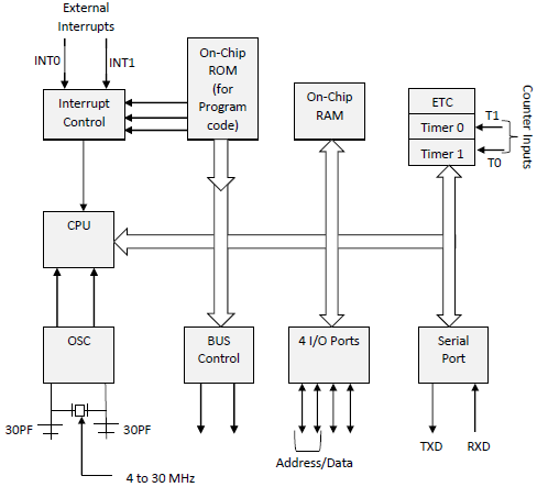
Let us now discuss the architecture of 8051 Microcontroller.
In the following diagram, the system bus connects all the support devices to the CPU. The system bus consists of an 8-bit data bus, a 16-bit address bus and bus control signals. All other devices like program memory, ports, data memory, serial interface, interrupt control, timers, and the CPU are all interfaced together through the system bus.
8051 Architecture

Microcontrollers - 8051 Pin Description

The pin diagram of 8051 microcontroller looks as follows −
8051 Pin Diagram
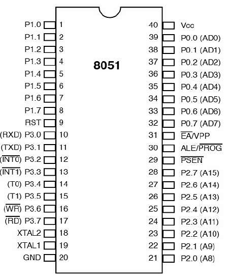
  • Pins 1 to 8 − These pins are known as Port 1. This port doesn’t serve any other functions. It is internally pulled up, bi-directional I/O port.
  • Pin 9 − It is a RESET pin, which is used to reset the microcontroller to its initial values.
  • Pins 10 to 17 − These pins are known as Port 3. This port serves some functions like interrupts, timer input, control signals, serial communication signals RxD and TxD, etc.
  • Pins 18 & 19 − These pins are used for interfacing an external crystal to get the system clock.
  • Pin 20 − This pin provides the power supply to the circuit.
  • Pins 21 to 28 − These pins are known as Port 2. It serves as I/O port. Higher order address bus signals are also multiplexed using this port.
  • Pin 29 − This is PSEN pin which stands for Program Store Enable. It is used to read a signal from the external program memory.
  • Pin 30 − This is EA pin which stands for External Access input. It is used to enable/disable the external memory interfacing.
  • Pin 31 − This is ALE pin which stands for Address Latch Enable. It is used to demultiplex the address-data signal of port.
  • Pins 32 to 39 − These pins are known as Port 0. It serves as I/O port. Lower order address and data bus signals are multiplexed using this port.
  • Pin 40 − This pin is used to provide power supply to the circuit.
  • Microcontrollers 8051 Input Output Ports

  • 8051 microcontrollers have 4 I/O ports each of 8-bit, which can be configured as input or output. Hence, total 32 input/output pins allow the microcontroller to be connected with the peripheral devices.
    • Pin configuration, i.e. the pin can be configured as 1 for input and 0 for output as per the logic state.
      • Input/Output (I/O) pin − All the circuits within the microcontroller must be connected to one of its pins except P0 port because it does not have pull-up resistors built-in.
      • Input pin − Logic 1 is applied to a bit of the P register. The output FE transistor is turned off and the other pin remains connected to the power supply voltage over a pull-up resistor of high resistance.
    • Port 0 − The P0 (zero) port is characterized by two functions −
      • When the external memory is used then the lower address byte (addresses A0A7) is applied on it, else all bits of this port are configured as input/output.
      • When P0 port is configured as an output then other ports consisting of pins with built-in pull-up resistor connected by its end to 5V power supply, the pins of this port have this resistor left out.

    Input Configuration

    If any pin of this port is configured as an input, then it acts as if it “floats”, i.e. the input has unlimited input resistance and in-determined potential.

    Output Configuration

    When the pin is configured as an output, then it acts as an “open drain”. By applying logic 0 to a port bit, the appropriate pin will be connected to ground (0V), and applying logic 1, the external output will keep on “floating”.
    In order to apply logic 1 (5V) on this output pin, it is necessary to build an external pullup resistor.

    Port 1

    P1 is a true I/O port as it doesn’t have any alternative functions as in P0, but this port can be configured as general I/O only. It has a built-in pull-up resistor and is completely compatible with TTL circuits.

    Port 2

    P2 is similar to P0 when the external memory is used. Pins of this port occupy addresses intended for the external memory chip. This port can be used for higher address byte with addresses A8-A15. When no memory is added then this port can be used as a general input/output port similar to Port 1.

    Port 3

    In this port, functions are similar to other ports except that the logic 1 must be applied to appropriate bit of the P3 register.

    Pins Current Limitations

    • When pins are configured as an output (i.e. logic 0), then the single port pins can receive a current of 10mA.
    • When these pins are configured as inputs (i.e. logic 1), then built-in pull-up resistors provide very weak current, but can activate up to 4 TTL inputs of LS series.
    • If all 8 bits of a port are active, then the total current must be limited to 15mA (port P0: 26mA).
    • If all ports (32 bits) are active, then the total maximum current must be limited to 71mA.
    • Microcontrollers - 8051 Interrupts
    • Interrupts are the events that temporarily suspend the main program, pass the control to the external sources and execute their task. It then passes the control to the main program where it had left off.
      8051 has 5 interrupt signals, i.e. INT0, TFO, INT1, TF1, RI/TI. Each interrupt can be enabled or disabled by setting bits of the IE register and the whole interrupt system can be disabled by clearing the EA bit of the same register.

      IE (Interrupt Enable) Register

      This register is responsible for enabling and disabling the interrupt. EA register is set to one for enabling interrupts and set to 0 for disabling the interrupts. Its bit sequence and their meanings are shown in the following figure.
      IE Register
      EAIE.7It disables all interrupts. When EA = 0 no interrupt will be acknowledged and EA = 1 enables the interrupt individually.
      -IE.6Reserved for future use.
      -IE.5Reserved for future use.
      ESIE.4Enables/disables serial port interrupt.
      ET1IE.3Enables/disables timer1 overflow interrupt.
      EX1IE.2Enables/disables external interrupt1.
      ET0IE.1Enables/disables timer0 overflow interrupt.
      EX0IE.0Enables/disables external interrupt0.

      IP (Interrupt Priority) Register

      We can change the priority levels of the interrupts by changing the corresponding bit in the Interrupt Priority (IP) register as shown in the following figure.
      • A low priority interrupt can only be interrupted by the high priority interrupt, but not interrupted by another low priority interrupt.
      • If two interrupts of different priority levels are received simultaneously, the request of higher priority level is served.
      • If the requests of the same priority levels are received simultaneously, then the internal polling sequence determines which request is to be serviced.
      IP Register
      -IP.6Reserved for future use.
      -IP.5Reserved for future use.
      PSIP.4It defines the serial port interrupt priority level.
      PT1IP.3It defines the timer interrupt of 1 priority.
      PX1IP.2It defines the external interrupt priority level.
      PT0IP.1It defines the timer0 interrupt priority level.
      PX0IP.0It defines the external interrupt of 0 priority level.

      TCON Register

      TCON register specifies the type of external interrupt to the microcontroller.

Friday 22 February 2019

UNIT - IV Peripheral Devices and I/O Interfacing

8259 PIC Microprocessor:

8259 microprocessor is defined as Programmable Interrupt Controller (PIC)microprocessor. There are 5 hardware interrupts and 2 hardware interrupts in 8085 and 8086 respectively. But by connecting 8259 with CPU, we can increase the interrupt handling capability. 8259 combines the multi interrupt input sources into a single interrupt output. Interfacing of single PIC provides 8 interrupts inputs from IR0-IR7.
For example, Interfacing of 8085 and 8259 increases the interrupt handling capability of 8085 microprocessor from 5 to 8 interrupt levels.
Features of 8259 PIC microprocessor –


  1. Intel 8259 is designed for Intel 8085 and Intel 8086 microprocessor.
  2. It can be programmed either in level triggered or in edge triggered interrupt level.
  3. We can masked individual bits of interrupt request register.
  4. We can increase interrupt handling capability upto 64 interrupt level by cascading further 8259 PIC.
  5. Clock cycle is not required.
Pin Diagram of 8259 –
We can see through above diagram that there are total 28 pins in 8259 PIC microprocessor where Vcc :5V Power supply and Gnd: ground. Other pins use are explained below.
Block Diagram of 8259 PIC microprocessor –


The Block Diagram consists of 8 blocks which are – Data Bus Buffer, Read/Write Logic, Cascade Buffer Comparator, Control Logic, Priority Resolver and 3 registers- ISR, IRR, IMR.
  1. Data bus buffer –
    This Block is used as a mediator between 8259 and 8085/8086 microprocessor by acting as a buffer. It takes the control word from the 8085 (let say) microprocessor and transfer it to the control logic of 8259 microprocessor. Also, after selection of Interrupt by 8259 microprocessor, it transfer the opcode of the selected Interrupt and address of the Interrupt service sub routine to the other connected microprocessor. The data bus buffer consists of 8 bits represented as D0-D7 in the block diagram. Thus, shows that a maximum of 8 bits data can be transferred at a time.
  2. Read/Write logic –
    This block works only when the value of pin CS is low (as this pin is active low). This block is responsible for the flow of data depending upon the inputs of RD and WR. These two pins are active low pins used for read and write operations.
  3. Control logic –
    It is the centre of the microprocessor and controls the functioning of every block. It has pin INTR which is connected with other microprocessor for taking interrupt request and pin INT for giving the output. If 8259 is enabled, and the other microprocessor Interrupt flag is high then this causes the value of the output INT pin high and in this way 8259 responds to the request made by other microprocessor.
  4. Interrupt request register (IRR) –
    It stores all the interrupt level which are requesting for Interrupt services.
  5. Interrupt service register (ISR) –
    It stores the interrupt level which are currently being executed.
  6. Interrupt mask register (IMR) –
    It stores the interrupt level which have to be masked by storing the masking bits of the interrupt level.
  7. Priority resolver –
    It examines all the three registers and set the priority of interrupts and according to the priority of the interrupts, interrupt with highest priority is set in ISR register. Also, it reset the interrupt level which is already been serviced in IRR.
  8. Cascade buffer –
    To increase the Interrupt handling capability, we can further cascade more number of pins by using cascade buffer. So, during increment of interrupt capability, CSA lines are used to control multiple interrupt structure.
SP/EN (Slave program/Enable buffer) pin is when set to high, works in master mode else in slave mode. In Non Buffered mode, SP/EN pin is used to specify whether 8259 work as master or slave and in Buffered mode, SP/EN pin is used as an output to enable data bus.

Block Diagram of 8259 Microprocessor:

  • 8259 microprocessor can be programmed according to given interrupts condition and it can be provided either with level or edge triggered interrupt level.
  • It can be programmed either work in 8085 or in 8086 microprocessors.
  • Individual interrupt bits can be masked.
  • By conducting more number of 8259 we can get upto 64 interrupt pins.
It contains 3 rigisters commonly known as ISR, IRR, IMR & there is 1 priority resolver (PR).
  1. Interrupt Request Register (IRR): It stores those bits which are requesting for their interrupt services.
  2. Interrupt Service Register (ISR): It stores that interrupt levels which is currently being servied.
  3. Interrupt Mask Register (IMR): It stores that interrupt levels which have to be masked. These interrupts levels are already acccepted by 8259 microprocessor.
Priority Resolver (PR): It examines all the 3 registers and set the priority of interrupts and set the interrupt levels in ISR which has highest priority and rest the interrupt bit is IRR which is already accepted.
SP/EN (low active pin): If its value is 1 it works in master mode & if its value=e is 0 then it works in slave mode.
Cascade Buffer: It is used to cascade more number of Programmable Interrupt Controller to increase the interrupts handling capability upto 64 level.

8279 - Programmable Keyboard

8279 programmable keyboard/display controller is designed by Intel that interfaces a keyboard with the CPU. The keyboard first scans the keyboard and identifies if any key has been pressed. It then sends their relative response of the pressed key to the CPU and vice-a-versa.

How Many Ways the Keyboard is Interfaced with the CPU?

The Keyboard can be interfaced either in the interrupt or the polled mode. In the Interrupt mode, the processor is requested service only if any key is pressed, otherwise the CPU will continue with its main task.
In the Polled mode, the CPU periodically reads an internal flag of 8279 to check whether any key is pressed or not with key pressure.

How Does 8279 Keyboard Work?

The keyboard consists of maximum 64 keys, which are interfaced with the CPU by using the key-codes. These key-codes are de-bounced and stored in an 8-byte FIFORAM, which can be accessed by the CPU. If more than 8 characters are entered in the FIFO, then it means more than eight keys are pressed at a time. This is when the overrun status is set.
If a FIFO contains a valid key entry, then the CPU is interrupted in an interrupt mode else the CPU checks the status in polling to read the entry. Once the CPU reads a key entry, then FIFO is updated, and the key entry is pushed out of the FIFO to generate space for new entries.

Architecture and Description

8279 Architecture

I/O Control and Data Buffer

This unit controls the flow of data through the microprocessor. It is enabled only when D is low. Its data buffer interfaces the external bus of the system with the internal bus of the microprocessor. The pins A0, RD, and WR are used for command, status or data read/write operations.

Control and Timing Register and Timing Control

This unit contains registers to store the keyboard, display modes, and other operations as programmed by the CPU. The timing and control unit handles the timings for the operation of the circuit.

Scan Counter

It has two modes i.e. Encoded mode and Decoded mode. In the encoded mode, the counter provides the binary count that is to be externally decoded to provide the scan lines for the keyboard and display.
In the decoded scan mode, the counter internally decodes the least significant 2 bits and provides a decoded 1 out of 4 scan on SL0-SL3.

Return Buffers, Keyboard Debounce, and Control

This unit first scans the key closure row-wise, if found then the keyboard debounce unit debounces the key entry. In case, the same key is detected, then the code of that key is directly transferred to the sensor RAM along with SHIFT & CONTROL key status.

FIFO/Sensor RAM and Status Logic

This unit acts as 8-byte first-in-first-out (FIFO) RAM where the key code of every pressed key is entered into the RAM as per their sequence. The status logic generates an interrupt request after each FIFO read operation till the FIFO gets empty.
In the scanned sensor matrix mode, this unit acts as sensor RAM where its each row is loaded with the status of their corresponding row of sensors into the matrix. When the sensor changes its state, the IRQ line changes to high and interrupts the CPU.

Display Address Registers and Display RAM

This unit consists of display address registers which holds the addresses of the word currently read/written by the CPU to/from the display RAM.

8279 − Pin Description

The following figure shows the pin diagram of 8279 −
8279 Pin Diagram

Data Bus Lines, DB0 - DB7

These are 8 bidirectional data bus lines used to transfer the data to/from the CPU.

CLK

The clock input is used to generate internal timings required by the microprocessor.

RESET

As the name suggests this pin is used to reset the microprocessor.

CS Chip Select

When this pin is set to low, it allows read/write operations, else this pin should be set to high.

A0

This pin indicates the transfer of command/status information. When it is low, it indicates the transfer of data.

RD, WR

This Read/Write pin enables the data buffer to send/receive data over the data bus.

IRQ

This interrupt output line goes high when there is data in the FIFO sensor RAM. The interrupt line goes low with each FIFO RAM read operation. However, if the FIFO RAM further contains any key-code entry to be read by the CPU, this pin again goes high to generate an interrupt to the CPU.

Vss, Vcc

These are the ground and power supply lines of the microprocessor.

SL0 − SL3

These are the scan lines used to scan the keyboard matrix and display the digits. These lines can be programmed as encoded or decoded, using the mode control register.

RL0 − RL7

These are the Return Lines which are connected to one terminal of keys, while the other terminal of the keys is connected to the decoded scan lines. These lines are set to 0 when any key is pressed.

SHIFT

The Shift input line status is stored along with every key code in FIFO in the scanned keyboard mode. Till it is pulled low with a key closure, it is pulled up internally to keep it high

CNTL/STB - CONTROL/STROBED I/P Mode

In the keyboard mode, this line is used as a control input and stored in FIFO on a key closure. The line is a strobe line that enters the data into FIFO RAM, in the strobed input mode. It has an internal pull up. The line is pulled down with a key closure.

BD

It stands for blank display. It is used to blank the display during digit switching.

OUTA0 – OUTA3 and OUTB0 – OUTB3

These are the output ports for two 16x4 or one 16x8 internal display refresh registers. The data from these lines is synchronized with the scan lines to scan the display and the keyboard.

Operational Modes of 8279

There are two modes of operation on 8279 − Input Mode and Output Mode.

Input Mode

This mode deals with the input given by the keyboard and this mode is further classified into 3 modes.
  • Scanned Keyboard Mode − In this mode, the key matrix can be interfaced using either encoded or decoded scans. In the encoded scan, an 8×8 keyboard or in the decoded scan, a 4×8 keyboard can be interfaced. The code of key pressed with SHIFT and CONTROL status is stored into the FIFO RAM.
  • Scanned Sensor Matrix − In this mode, a sensor array can be interfaced with the processor using either encoder or decoder scans. In the encoder scan, 8×8 sensor matrix or with decoder scan 4×8 sensor matrix can be interfaced.
  • Strobed Input − In this mode, when the control line is set to 0, the data on the return lines is stored in the FIFO byte by byte.

Output Mode

This mode deals with display-related operations. This mode is further classified into two output modes.
  • Display Scan − This mode allows 8/16 character multiplexed displays to be organized as dual 4-bit/single 8-bit display units.
  • Display Entry − This mode allows the data to be entered for display either from the right side/left side.
  • Microprocessor - 8257 DMA Controller

DMA stands for Direct Memory Access. It is designed by Intel to transfer data at the fastest rate. It allows the device to transfer the data directly to/from memory without any interference of the CPU.
Using a DMA controller, the device requests the CPU to hold its data, address and control bus, so the device is free to transfer data directly to/from the memory. The DMA data transfer is initiated only after receiving HLDA signal from the CPU.

How DMA Operations are Performed?

Following is the sequence of operations performed by a DMA −
  • Initially, when any device has to send data between the device and the memory, the device has to send DMA request (DRQ) to DMA controller.
  • The DMA controller sends Hold request (HRQ) to the CPU and waits for the CPU to assert the HLDA.
  • Then the microprocessor tri-states all the data bus, address bus, and control bus. The CPU leaves the control over bus and acknowledges the HOLD request through HLDA signal.
  • Now the CPU is in HOLD state and the DMA controller has to manage the operations over buses between the CPU, memory, and I/O devices.

Features of 8257

Here is a list of some of the prominent features of 8257 −
  • It has four channels which can be used over four I/O devices.
  • Each channel has 16-bit address and 14-bit counter.
  • Each channel can transfer data up to 64kb.
  • Each channel can be programmed independently.
  • Each channel can perform read transfer, write transfer and verify transfer operations.
  • It generates MARK signal to the peripheral device that 128 bytes have been transferred.
  • It requires a single phase clock.
  • Its frequency ranges from 250Hz to 3MHz.
  • It operates in 2 modes, i.e., Master mode and Slave mode.

8257 Architecture

The following image shows the architecture of 8257 −
8257 Architecture

8257 Pin Description

The following image shows the pin diagram of a 8257 DMA controller −
8257 Pin Diagram

DRQ0−DRQ3

These are the four individual channel DMA request inputs, which are used by the peripheral devices for using DMA services. When the fixed priority mode is selected, then DRQ0 has the highest priority and DRQ3 has the lowest priority among them.

DACKo − DACK3

These are the active-low DMA acknowledge lines, which updates the requesting peripheral about the status of their request by the CPU. These lines can also act as strobe lines for the requesting devices.

Do − D7

These are bidirectional, data lines which are used to interface the system bus with the internal data bus of DMA controller. In the Slave mode, it carries command words to 8257 and status word from 8257. In the master mode, these lines are used to send higher byte of the generated address to the latch. This address is further latched using ADSTB signal.

IOR

It is an active-low bidirectional tri-state input line, which is used by the CPU to read internal registers of 8257 in the Slave mode. In the master mode, it is used to read data from the peripheral devices during a memory write cycle.

IOW

It is an active low bi-direction tri-state line, which is used to load the contents of the data bus to the 8-bit mode register or upper/lower byte of a 16-bit DMA address register or terminal count register. In the master mode, it is used to load the data to the peripheral devices during DMA memory read cycle.

CLK

It is a clock frequency signal which is required for the internal operation of 8257.

RESET

This signal is used to RESET the DMA controller by disabling all the DMA channels.

Ao - A3

These are the four least significant address lines. In the slave mode, they act as an input, which selects one of the registers to be read or written. In the master mode, they are the four least significant memory address output lines generated by 8257.

CS

It is an active-low chip select line. In the Slave mode, it enables the read/write operations to/from 8257. In the master mode, it disables the read/write operations to/from 8257.

A4 - A7

These are the higher nibble of the lower byte address generated by DMA in the master mode.

READY

It is an active-high asynchronous input signal, which makes DMA ready by inserting wait states.

HRQ

This signal is used to receive the hold request signal from the output device. In the slave mode, it is connected with a DRQ input line 8257. In Master mode, it is connected with HOLD input of the CPU.

HLDA

It is the hold acknowledgement signal which indicates the DMA controller that the bus has been granted to the requesting peripheral by the CPU when it is set to 1.

MEMR

It is the low memory read signal, which is used to read the data from the addressed memory locations during DMA read cycles.

MEMW

It is the active-low three state signal which is used to write the data to the addressed memory location during DMA write operation.

ADST

This signal is used to convert the higher byte of the memory address generated by the DMA controller into the latches.

AEN

This signal is used to disable the address bus/data bus.

TC

It stands for ‘Terminal Count’, which indicates the present DMA cycle to the present peripheral devices.

MARK

The mark will be activated after each 128 cycles or integral multiples of it from the beginning. It indicates the current DMA cycle is the 128th cycle since the previous MARK output to the selected peripheral device.

Vcc

It is the power signal which is required for the operation of the circuit.

UNIT - V 8051 Microcontroller

Microcontrollers - 8051 Architecture 8051 microcontroller is designed by Intel in 1981. It is an 8-bit microcontroller. It is built wit...